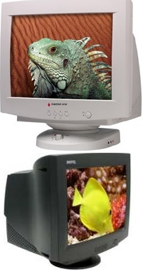
Mitsubishi Diamond View and BenQ - 17" CRT Monitors. Used ICs: LM1269
– LM2467 – UC3842B – TW10N70Z(FET) – MY87C52 – BU2527AF(Horizontal output
transistor) – 19.70065.001(LOT) – TDA4856 – TDA4866(Vertical Scan Out IC)
Vertical
Output Circuit
This vertical driver IC circuit is a bridge configuration
The signals from TDA4856 differential output VOUT1 and VOUT2 are connected to TDA4866 via DC-Coupled.
The vertical deflection coil is connected between the output amplifier (TDA 4866 pin4 and Pin6 ) ,Which are driven in phase opposite . The TDA4866 can output current to drive vertical deflection yoke .
PIN8 ( GUARD) is used for vertical blanking.
The
current mode control IC UC3842 is used in the switching power supply which
function of each pin described as follows.
pin
1 : Error amplifier output
pin
2 : Error amplifier reverse input
pin
3 : Current sense
pin
4 : OSC sawtooth
pin
5 : Ground
pin
6 : Output
pin
7 : VCC
pin
8 : Reference Voltage:5V
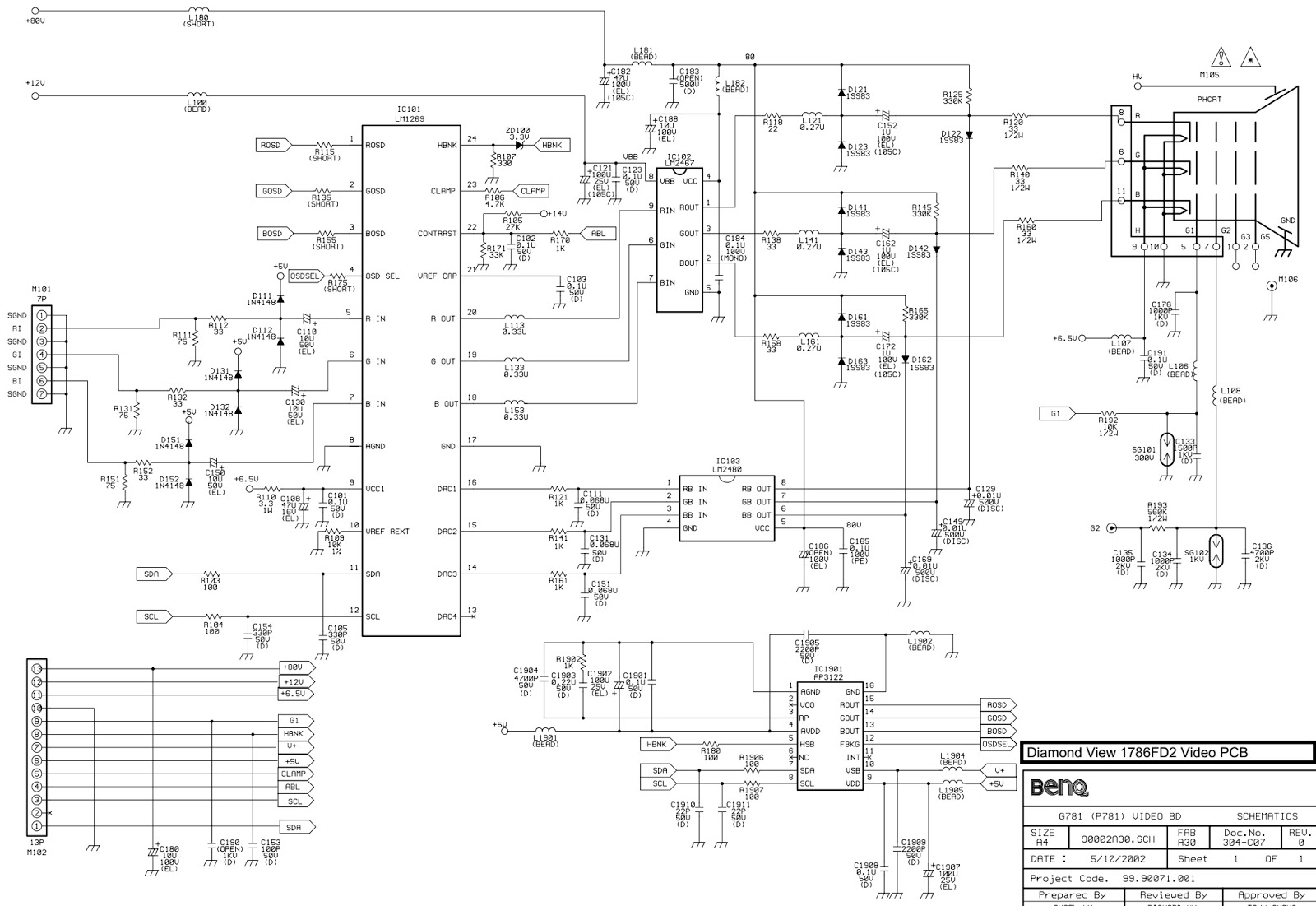
Circuit Diagram (Schematic)
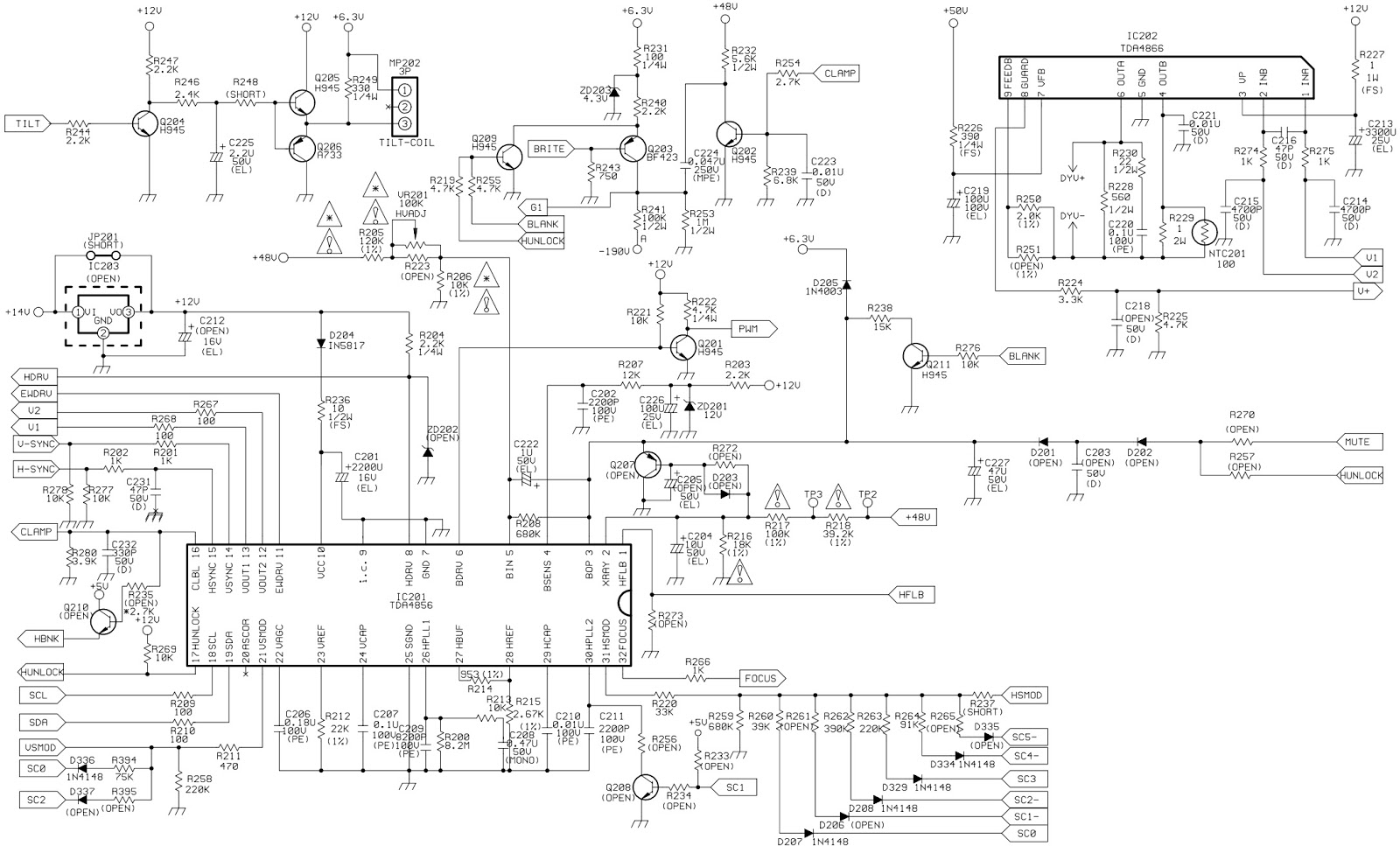


When power is initially applied to the circuit, capacitor C626 charges through R624, R623, ZD601. When the voltage across C607 reaches a level of 16V, IC601 is turn-on the +5Vdc will be set up at pin8 then R613, C615 generate a fixed frequency sawtooth wave to pin4, at this time MOSFET will be drived by pin6 with square wave the pulse width of square wave is decided by pin2 , pin3 is current feedback control, It will to sense MOSFET current. The D613, D612, R614, C617 are soft start components to avoid the duty too large when power starts up.
Feedback circuit: This power supply adopt feedback circuit of +45V and +13V. It used IC702 for voltage regulation and IC602 for primary-secondary isolation, The output voltage differential signal will be detected and sensed to the pin2 of UC3842 for comparison then the duty cycle of MOSFET will be decided to control the output voltage.
CRT DRIVER CKT: Output stage adopts CRT driver LM2439 to amplify the signal which has been recessed by LM1279 to a enough amplitude of Vpp, then display on the CRT. The IC contains three high input impedance, wide band amplifiers which directly drive the RGB cathodes of a CRT. The gain of each channel is internally set at -15 and can drive CRT capacitive loads as well as resistive loads presented by other application limited only by the package’s power dissipation.
DC Restore CKT:
(a) The video signal amplified by the output stage is coupled to CRT by way of AC coupling. SO DC restoration CKT is needed to do the white balance adjustment.
(b) This DC restoration circuit adopts SYNC TIP CLAMP, In the duration of SYNC TIP the capacitor charges, and the capacitor discharge in the other time. The Black Level is kept to the level of DC restoration settled by UC.
ABL CKT: (Auto Brightness Limit) ABL is a protection circuit. When the anode current goes higher than the setting value of ABL circuit . ABL will pull down the voltage of contrast to limit the anode current. This is helpful to protect CRT.
H-BLANK CKT: Affair the collect pulse comes from FBT being shaped and inverted, it will be sent to preamp CKT and used as the H-Blank.
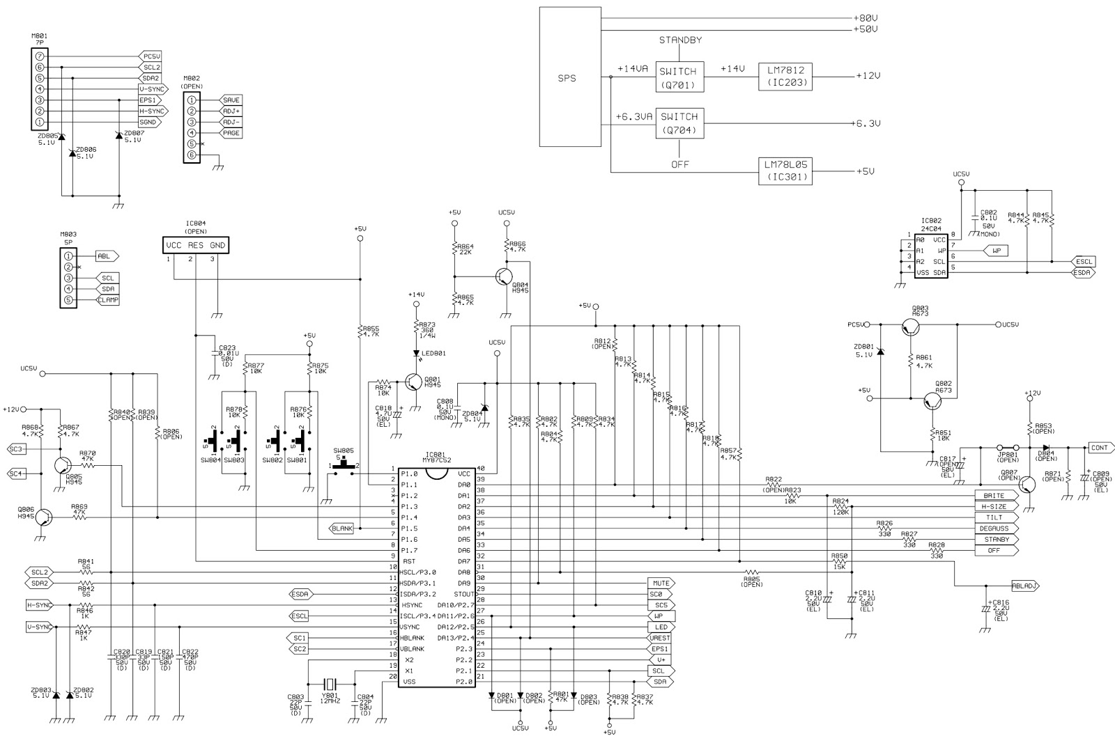
Brightness,
V-blank, change mode blank, spot-killer CKT:
(a)
About the cut off voltage, while the voltage, cathode to G1 , over the cut off
, voltage, the picture will disappear, If cut off voltage off the CRT G Gru is settled
at 110V and the black level of cathode is 60v, the picture won’t show, the
signals higher the black level once the G1 voltage is lower than-50v.
(b)
As described above, we may use the voltage control G1 as the brightness
control. Generally the G1 control range is about 10~15V if the raster
brightness is form 0 to 1.5 ft-L.
(c)
Similarly, we may overlap a negative pulse of vertical duration on the G1
voltage to prevent the vertical retrace line from showing on the picture; this
is to keep the voltage cathode to G1 over the cut off voltage during the period
of vertical retrace.
(d)
In order to avoid the picture occur transiently while change mode, pull down
the G1 voltage and let the voltage cathode to G1 over CUT OFF voltage. This
will make the picture blanking.
(e)
While monitor turned off, the discharge speed of high voltage circuit is slow
since there is no deflection scan act on the electronic beam, a spot which will
destroy the phosphor of CRT. So the SPOT KILLER circuit will generate a negative
voltage higher than CUT OFF to the G1 to beam this is to protect the CRT.
Video
board
Caution: Before power on, you must check whether all connectors and components of the set are correct, otherwise it maybe to destroy the set. There assume that following cases depend on above setup OK. Please follow as below and check it step by step.
Caution: Before power on, you must check whether all connectors and components of the set are correct, otherwise it maybe to destroy the set. There assume that following cases depend on above setup OK. Please follow as below and check it step by step.
No
video display on screenCheck IC101 pin 10 (Video Contrast). If it is 0 volt, check IC1901 or maybe
IC101 pin 10 short.Check IC101 pin 18,15,13 If they are 0 volts, replace a new IC to IC101.Check RGB cathode. If anyone pin is 0 volt, replace a new IC to IC102.Check IC102 output path. It must be right and without short circuit.Check G1 voltage. If it is lower equal than -182 volts, check spot killer
circuit and check IC801 pin6(Blank).Check CRT heater. If it is dark, check +8v supply voltage of heater.Replace CRT if it burns out.
One
or more of R, G, B channel does no display
Check IC101 pin 18,15,13. If anyone is 0 volt, replace a new IC to IC101.Check RGB cathode. If anyone pin is 0 volt, replace a new IC to IC102.Check IC102 output path. It must be right and without short circuit.Replace CRT if it burns out.
Check IC101 pin 18,15,13. If anyone is 0 volt, replace a new IC to IC101.Check RGB cathode. If anyone pin is 0 volt, replace a new IC to IC102.Check IC102 output path. It must be right and without short circuit.Replace CRT if it burns out.
OSD does not display on screen
Check IC101 pin 1,19,20. If they are 0 volt, check IC101 and IC1901.
No video display on screen, but OSD can display on screen
Check IC101 pin 10 (Video Contrast). If it is 0 volt, check IC1901 or maybe IC101 pin 10 short.
OSD control cannot adjust Bias
Check IC1901.
Check DC restore circuit.
OSD control cannot adjust Drive
Check IC101 and IC1901.
OSD control cannot adjust Contrast
Check IC 101 and IC1901.
OSD control cannot adjust Brightness
Check brightness control circuit (G1) and IC801 BRITE output.
ABL cannot adjust
Check ABL circuit.
Spot killer function failure
Check SG101(300KV spark gap). Replace it if it is inserted error.
check spot killer circuit.
Picture quality is not so good
Check CRT socket. Fix it if it is loose.
Check IC101 pin 11(clamp gate). If it has no clamping pulse, check H-clamp pulse switch circuit.
Replace IC102.
Moire appears when Y is greater than 18 Ft-l
Run auto-alignment procedure to acquire optimum G2 voltage.
If necessary, decrease G2 voltage.
H-blank function failure
Check H-blank circuit