Monday, September 30, 2013

HOW TO EXCHANGE LBE - LBF & LBG BOARDS TO A PLASMA DISPLAY

LBG / LBF / LBE Boards replacement
CLICK ON THE PICTURES TO ZOOM
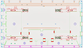
  • Remove the screws in order of 2-3-5-7-1-4 from heat sink and then get rid of heat sink.
  • Remove the TPC, FFC and power cable from the connectors.
  • Remove all of the screws from defected board.
  • Remove the defective board.
  • Replace the new board and then screw tightly.
  • Get rid of the foreign material from the connector.
  • Connect the TCP,FFC and power cable to the connector.
  • Reassemble the TCP heat sink.
  • Screw in order of 4-1-7-6-5-3-2.

Exchange YBU, YBL and YM board.
  • Separate all of the FPC connector of YBU (Y-Buffer upper) and YBL (Lower).
  • Separate all of the connector of CN5001 and CN5008 from Y-Main.
  • Loosen all of the screws of YBU, YBL and YM.
  • Remove the board from chassis.
  • Remove the connector of CN5006 and CN5007 among YBU, YBL and YM.
  • Remove the YBL and YBU from Y-main.
  • Replace the defective board.
  • If you screw too tightly, it is possible to get damage on the Driver IC of TCP.
Reassemble the YBU and YBL to the Y-Main.
Connect the connector of CN5006 and CN5007 among YBU, YBL and YM.
Arrange the board on the chassis and then screw to fix.
Connect the FPC and YM of panel to the connector.
Supply the electric power to the module and then check the waveform of board.
Turn off the power after the waveform is adjusted

HOW TO DISASSEMBLE & REASSEMBLE BOARDS TO A PLASMA DISPLAY


DISASSEMBLING & REASSEMBLING
Disassembling & Re-assembling of FPC (Flexible Printed Circuit) and Y-Buffer(Upper and Lower).
Removal procedures.
Full out the FPC from Connector by holding the lead of the FPC with hands.
CLICK ON THE PICTURES TO ZOOM
Assembling Procedures.
Push the lead of FPC with same strength until to be connected completely.
Note: Be careful do not get a damage on the connector pin during connecting by mistake.
Assembling & Disassembling of Flat Cable Connector of X-Main Board.
Disassembling Procedure.
Pull out the clamp of connector.
Pull Flat cable out press down lightly.
Turn the Flat cable reversal.
Assembling Procedure.
Put the Flat cable into the connector press down lightly until locking sound (“Dack”) comes out.
Assembling & Disassembling the FFC and TCP from Connector.
Disassembling of TCP
Open the clamp carefully.
Pull the TCP out from Connector.
Assembling of TCP
Put the TCP into the Connector carefully.
Close the clamp completely. ( The sound (“ Dack”) comes out.)
Notes : TCP and Connector was connected surely.
Checking whether the foreign material is on the Connector inside before assembling of TCP.
Be careful do not get a damage on the board by ESD during handling of TCP.
Misassembling of TCP
The misassembled of TCP is the cause of defect.
Checking method of misassembled of TCP.
  • Disconnecting H3 from CN8006 of LBE.
  • Whether H8 and H9 are connected.
  • Checking the resistance between Pin 1 and 5.
  • Resistance > a few [ KOhm] :OK
  • Resistance < 20 Ohm : At least, more than 1pc of TCP is wrong.
Assembling & Disassembling of FFC
The procedure of assembling and disassembling of FFC is the same as TCP.

PLASMA TVs _DEFECTS & SYMPTOMS

Symptoms & Possible Reasons
F/White low discharge.
  • Low discharge caused by unstable cells occurring at full white pattern if high (60 degree) or normal temperature.
  • Panel: MgO source / dielectric thickness cell pitch/phosphor.
  • Circuit: drive waveform/ voltage condition.
Weak discharge.
  • Normal discharge but cells appear darker due to weak light emission occurring mainly at low (5 degree) Full white/Red/Green/Blue pattern or gradation pattern.
  • Panel : MgO deposition count and thickness / aging condition.
  • Circuit: drive waveform/ voltage condition.
Exhaust pipe damage.
Crack in break if exhaust pipe an image is partially lacking or the panel noise occurs depending on the damaged parts and with the passage of time.

DEFECTS_SYMPTOMS & DEFECTIVE PARTS _ PLASMA TVs_DEFECTIVE SCREEN SHOTS

PLASMA DISPLAY DEFECTS
No Voltage Output
Operating Voltages don't exist.

PSU [Power Supply Unit]

No Display
Operating Voltages exist, but an Image doesn't exist on screen

Y-MAIN, X-MAIN, Logic Main, Cables

Abnormal Display
Abnormal image (not open or short) is on screen.

Y-MAIN, X-MAIN, Logic Main
Sustain Open
Some horizontal lines don't exist on screen

Scan Buffer, FPC of X/ Y

Sustain Short
Some horizontal lines appear to be linked on screen


Scan Buffer, FPC of X/ Y
Address Open
Some vertical lines don't exist on screen

Logic Main, Logic Buffer, FFC,TCP

Address Short
Some vertical lines appear to be linked on screen
Logic Main, Logic Buffer, FFC, TCP
A line or block does not light up in address electrode direction. (1 line, block open).
Manufacturing: Panel electrode single line/ foreign material./electrostatic/ TCP defect.
Another color simultaneously appears because adjacent data recognizes the single pattern signal.
Manufacturing: Panel electrode short/ Foreign material conductive foreign object inside TCP.
A defect other than address open and short Data printout signal error occurring at certain Gradation or pattern.
One or more line do not light up in Sustain direction.
  • Manufacturing:. Panel bus electrode single line FPC pressure defect.
  • Parts: FPC/board/connection disconnection
  • Operation: assembly error.
Sustain (horizontal stripe) Short.
Combined or adjacent lines are short in sustain direction. The line appears brighter than other at Ramp gradation pattern or low gradation pattern.
Dielectric material layer damage.
Burn caused by the damage of address bus dielectric layer appears in the panel discharge/non discharge area. sustain also open/short occurs by the damage of address sustain printout. [Add Block and Line Open]
  • Manufacturing: Panel electrode short/Foreign material.
  • Parts: Board/ connector/pin error
  • Operation: connector / assembling error.
Add and Sustain Open.
Layer uneven / abnormal voltage / foreign material repair failed.

DEFLECTION_SCHEMATIC (Circuit diagram) _HITACHI PTV- 43 / 51 / 57


DEFLECTION SCHEMATIC
  • All DC voltage to be measured with a tester (100kOHms/V). Voltage taken on a complex color bar signal including a standard color bar signal.
  • Since this is a basic circuit diagram, the value of the parts is subject to be altered for improvement.

PRODUCT SAFETY NOTE: Components marked with a and shaded have special characteristics important to safety. Before replacing any of these components

CLICK ON THE SCHEMATIC TO ZOOM

HITACHI PTV - 43FWX20B - HOW TO DISASSEMBLE


DISASSEMBLY PROCEDURE
The Front Speaker Grille needs to be removed.
Remove 4 Screws located on the back sides of the Speaker Grille (2 on each side).
The image on the right shows the 2 screws on the right back side of the Speaker Grille.
The image shows the Speaker Grille removed.

The Lower Rear board needs to be removed. Remove 14 screws all around the Lower Rear Board.
Image shows Lower Rear Board removed.
Next to be removed is the Back Cover, which is partially shown in this image.
Remove the 18 screws all around the Back Cover.
The image shows the back of the right side of the Back Cover.
Again, use extreme caution because the mirror is attached to the Back Cover.
Image shows the back of the PTV with the Back Cover and Lower Rear Board removed.
Look for the Sensor Board located on the top right corner. Remove the Sensor Interface connectors.
Remove the 4 screws (2 on each corner) that partially hold the screen frame assembly.
Image shows the 2 screws on the right corner near the sensor board.
Locate and remove the last 7 screws on the bottom edge on the front of the Screen Frame. (2 on each corner and 3 in the center.)
The image shows the bottom edge of the screen frame.
Note that these screws are the last ones that are holding the Screen Frame. Grab the Screen Frame on both corners and slide out towards you.
Seek additional help when necessary.
This image shows the PTV after you have removed the Screen Frame assembly.
CLICK ON THE IMAGES TO ZOOM

Sunday, September 29, 2013

RPTV_HITACHI_51/57UWX20B_51/57GWX20B - HOW TO DISASSEMBLE - SCREEN FRAME&LIGHTBOX


The following instructions are for models with lightbox design. The new cabinet design will enable to remove the light box assembly, without taking complete PTV out for service.
Remove the Front Speaker Grille.
Pull the Speaker Grille off by placing your hand behind the outside corners and pulling straight out.
The bottom picture shows the TV after the Speaker Grille has been removed.
Remove the screws on the left bottom corner of the screen frame.

Remove the screws on the right bottom corner of the screen frame.
Remove the screen assembly by placing your hands on corners and lifting up to unhook from the cabinet.
Use additional help when necessary.
Carefully store Screen Frame Assembly.
After taking off the screen assembly, the cabinet light cavity will be exposed.
Remove the 4 screws on the left of the CRT Lens assembly.
Remove the 4 screws on the right of the CRT Lens assembly.
Now move to the back of the PTV. The lower rear board must be removed.
Remove 14 screws to remove the lower rear board.
Now, move to the chassis area on the back of the TV.
Remove the 3 screws to the right of the chassis as shown.
Remove one screw on the left of the chassis as shown.
Remove the screw on the right corner of the light box.
Remove the screw on the left corner of the light box.
Remove the screws on the front that hold the light box.
The picture shows the right side.
Remove the screws on the front that hold the light box.
The picture shows the left side.
Remove the control panel.
Remove the board on top of the light box assembly.
Lift the Light box in the center and slide backwards until it is out. Use additional help if necessary.
The Light Box is now ready for easy transport to a designated service and repair facility.