Panel screen: LTA260AP02, Panel screen: LTA320AB02 and LTF320AB01, PANEL SCREEN: LTJ400HM03 B
Panel
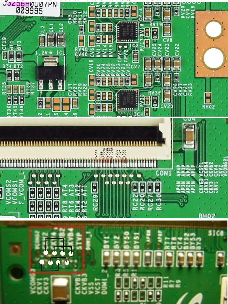
screen: LTA260AP02, T-CON 260AP02C2LV0.2, Level Shifter-IC8-AG32AE2
Level shifter receives from processor this low voltage signals: OE, STV and CPV1, CPV2, and from DC-DC source, VON and VOFF voltages
Output signals that controls 2 gate drivers are CKV1, CKVB1 and STVP1, respectively, CKV2, CKVB2 and STVP2
Level shifter receives from processor this low voltage signals: OE, STV and CPV1, CPV2, and from DC-DC source, VON and VOFF voltages
Output signals that controls 2 gate drivers are CKV1, CKVB1 and STVP1, respectively, CKV2, CKVB2 and STVP2
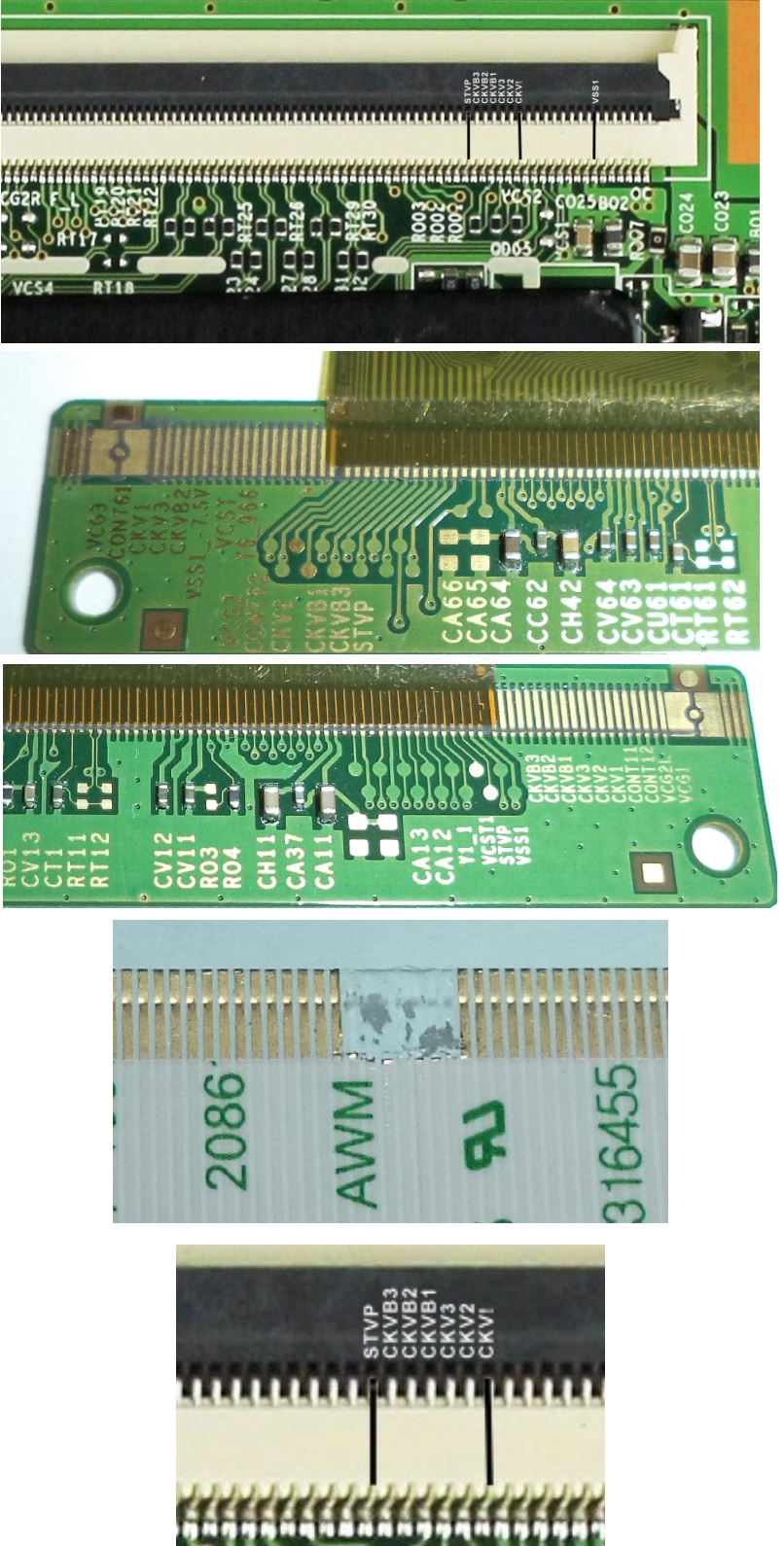
Clock
signals are starting from T-con Board, and you don't have to open the screen
panel. First, cut and disconnect on printed side, where indicated in picture,
CKV1 and CKVB1, strap on the check point on component side only CKV1 and CKVB1.
If
still image fault, proceed identical with CKV2 and CKVB2. If there is no image,
just rebuild the CKV1 and CKVB1 connections on printed side. Sometimes, you
need to disconnect also STVP1 (2) signal. Be patience, and check all
combinations possible to have a normal picture. If fault solved but after a
while appears some vertical white lines in an area with a static image, like a
channel logo, you have to connect strapped pair to VOFF, instead of GND, and
raise a little the VOFF with minus 3-5v. You can do that by lowering the
resistor connected between REF and FBN of bias power supply IC7. Have TPS65160
schematic below.
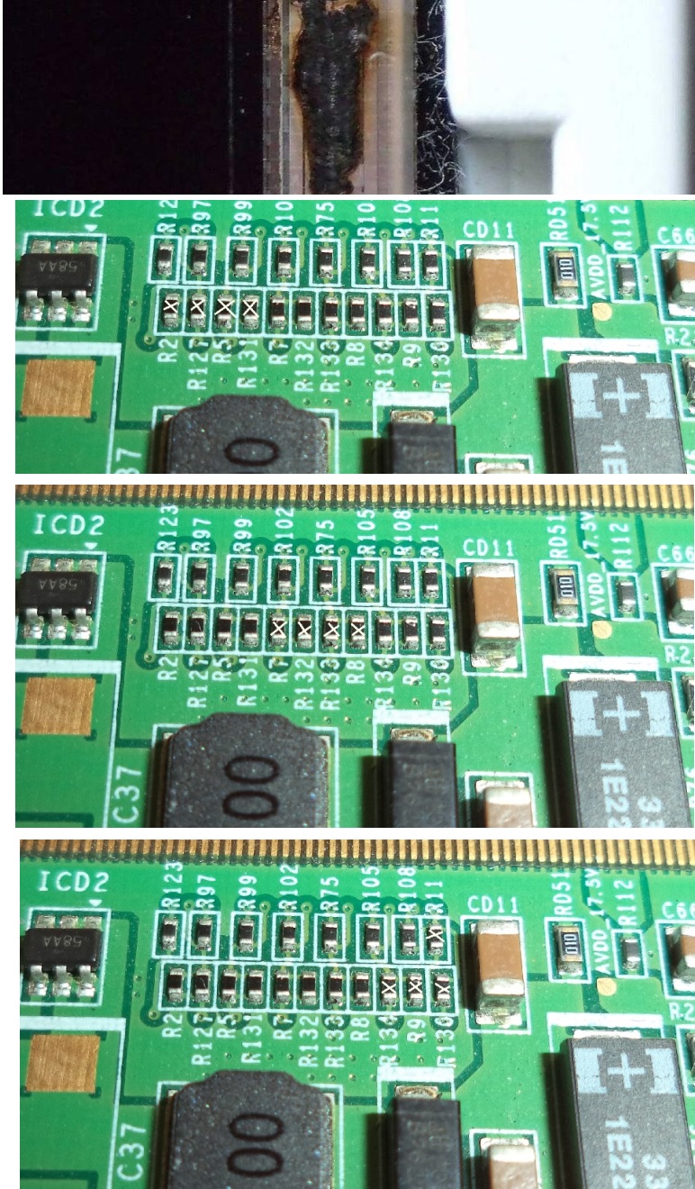
Another
fault, over all image there are vertical thin colored lines.
All voltages are correct. SDRAM – IC4 EM638325TS-7G is fault. Change T-con or replace memory.
All voltages are correct. SDRAM – IC4 EM638325TS-7G is fault. Change T-con or replace memory.
Another
fault – black screen, after a while will appear vertical colored lines. Check
all voltages – AVDD, VCC, VON, VOFF. Usually there is a problem with Von
voltage, bias power supply TPS65160 fault. Change T-con or replace IC.
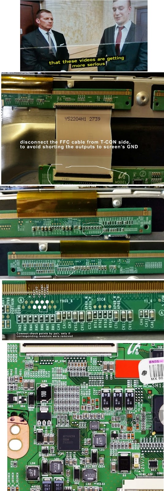
Panel screen: LTA320AB02 and LTF320AB01, T-CON 320AB02CP2LV0.3, Level Shifter-2x AG16BG
On this panels, we have 2 versions of repairing it.
1) on T-con board: There are 2 gate drivers and clock signals are outputted by 2 level shifter IC's, ICS1 and ICS2, located on T-con board
First, cut the circuits between ICS1 - CKV1 and CKVB1, right near resistors, as shown in image below. If image still fault, try to strap CKV1 and CKVB1, connect to the ground, or connect with an wire to Voff. ATTENTION! Make sure the connection between check point and ICS1 is opened with diode instrument, before strapping CKV1 and CKVB1. If there is still connection to the level shifter IC, you can burn it by connecting to the ground or Voff.
If image still faults, make a similar procedure with ICS2, by disconnecting CKV2 and CKVB2. Reconnect CKVB1 and CKVB2 to ICS1, and follow the same procedure.
If image is correct, but on still images there are some white vertical artefacts, you have to connect strapped pair to VOFF, instead of GND.
2) on PWB connected to glass screen panel Cut the connections CKV1, CKVB1, CKV2, CKVB2 and STVP1 (2) on side with gate block fault (left or right) . You can see where is the fault, by checking left/right margin of the screen with a magnifier lens, or a microscope. You will see a burned glass circuit, in the area where screen faults.

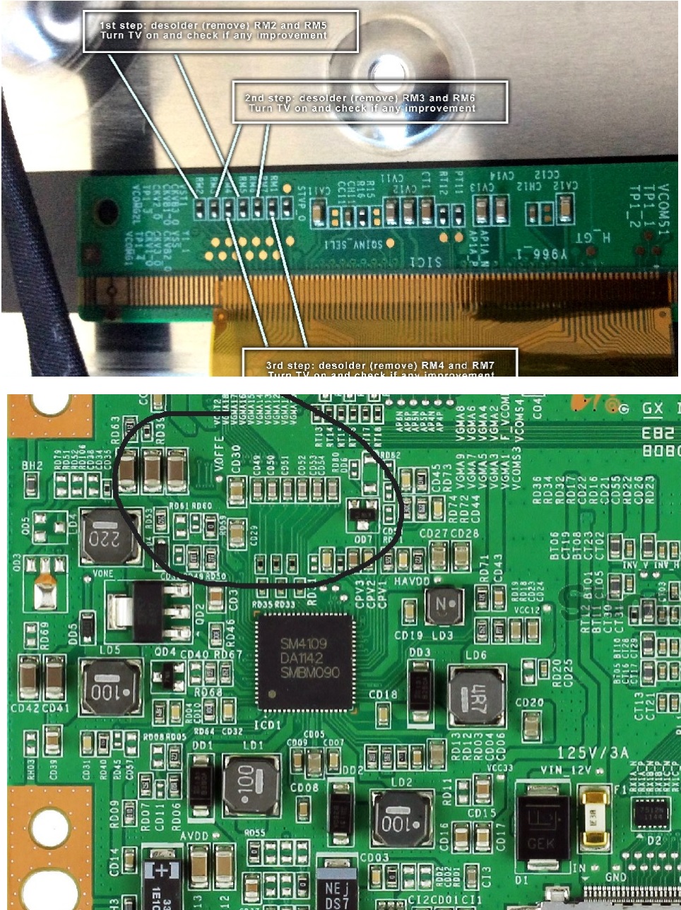
PANEL SCREEN: LTJ400HM03 B, T-Con S100FAPC2LV0.3
Screen is flickering; have a part/all the screen with doubled image.
First step is to find which part of the screen is fault. Disconnect left FFC between Tcon and left PWB and power the tv. If you have now on right part of the screen a normal image, means that you have a fault in left side of the cell. If still a fault image, re-connect the left FFC and disconnect right FFC between T-con and left PWB and power the tv. If you have now on left part of the screen a normal image, means that you have a fault in right side of the cell. On the right side (with problems) just remove the CKV1 and CKVB1 resistors RM2 and RM5 and see any improvements.
If not, remove CKV2 and CKVB2 resistors RM2 and RM6, check if any improvements, and if not, remove CKV3 and CKVB3 resistors RM3 and RM7. If still no improvements, remove STVP resistor, RM1 see picture.
You will have a normal picture now, but sometimes, you will have, on side with problems, a little ODD/EVEN lines distance. Strap with a wire, on check points, CKV1 with CKVB1, see if lines are now correct displayed. If not, strap with a wire, on check points, CKV2 with CKVB2, check, and repeat procedure with CKV3 with CKVB3. Now you will have a clean image. Sometimes, will be better to put back the resistors for the blocks pair that have no problem. For example if only by disconnecting CKV3 and CKVB3 will solve image problem, that means pair 1 and 2 have no problems. Sometimes, if you have a bigger problem on cell circuit, the image will be correct but a / some thin line (s) will be displayed sometimes on screen, noticeable on lighter/darker images. Try to connect the strapped pair that not work on GND or Voff. You can also raise Voff voltage with 3-5 volts to minus and the line will disappear. You can do that by changing the input resistors from FBN input of BiasPS/Level shifter ICD1 – SM4109