Saturday, December 30, 2017

How to repair Samsung LCD TV panel screen - Part 5 of 5

Panel screen: LTA260AP02, Panel screen: LTA320AB02 and LTF320AB01, PANEL SCREEN: LTJ400HM03 B
Panel screen: LTA260AP02, T-CON 260AP02C2LV0.2, Level Shifter-IC8-AG32AE2
Level shifter receives from processor this low voltage signals: OE, STV and CPV1, CPV2, and from DC-DC source, VON and VOFF voltages
Output signals that controls 2 gate drivers are CKV1, CKVB1 and STVP1, respectively, CKV2, CKVB2 and STVP2
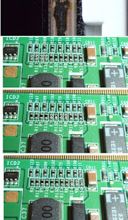
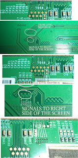
Clock signals are starting from T-con Board, and you don't have to open the screen panel. First, cut and disconnect on printed side, where indicated in picture, CKV1 and CKVB1, strap on the check point on component side only CKV1 and CKVB1.
If still image fault, proceed identical with CKV2 and CKVB2. If there is no image, just rebuild the CKV1 and CKVB1 connections on printed side. Sometimes, you need to disconnect also STVP1 (2) signal. Be patience, and check all combinations possible to have a normal picture. If fault solved but after a while appears some vertical white lines in an area with a static image, like a channel logo, you have to connect strapped pair to VOFF, instead of GND, and raise a little the VOFF with minus 3-5v. You can do that by lowering the resistor connected between REF and FBN of bias power supply IC7. Have TPS65160 schematic below.
Another fault, over all image there are vertical thin colored lines.
All voltages are correct. SDRAM – IC4 EM638325TS-7G is fault. Change T-con or replace memory.
Another fault – black screen, after a while will appear vertical colored lines. Check all voltages – AVDD, VCC, VON, VOFF. Usually there is a problem with Von voltage, bias power supply TPS65160 fault. Change T-con or replace IC.
Panel screen: LTA320AB02 and LTF320AB01T-CON 320AB02CP2LV0.3, Level Shifter-2x AG16BG
On this panels, we have 2 versions of repairing it.
1) on T-con board: There are 2 gate drivers and clock signals are outputted by 2 level shifter IC's, ICS1 and ICS2, located on T-con board
First, cut the circuits between ICS1 - CKV1 and CKVB1, right near resistors, as shown in image below. If image still fault, try to strap CKV1 and CKVB1, connect to the ground, or connect with an wire to Voff. ATTENTION! Make sure the connection between check point and ICS1 is opened with diode instrument, before strapping CKV1 and CKVB1. If there is still connection to the level shifter IC, you can burn it by connecting to the ground or Voff.
If image still faults, make a similar procedure with ICS2, by disconnecting CKV2 and CKVB2. Reconnect CKVB1 and CKVB2 to ICS1, and follow the same procedure.
If image is correct, but on still images there are some white vertical artefacts, you have to connect strapped pair to VOFF, instead of GND.
2) on PWB connected to glass screen panel Cut the connections CKV1, CKVB1, CKV2, CKVB2 and STVP1 (2) on side with gate block fault (left or right) . You can see where is the fault, by checking left/right margin of the screen with a magnifier lens, or a microscope. You will see a burned glass circuit, in the area where screen faults.
PANEL SCREEN: LTJ400HM03 B, T-Con S100FAPC2LV0.3
Screen is flickering; have a part/all the screen with doubled image.
First step is to find which part of the screen is fault. Disconnect left FFC between Tcon and left PWB and power the tv. If you have now on right part of the screen a normal image, means that you have a fault in left side of the cell. If still a fault image, re-connect the left FFC and disconnect right FFC between T-con and left PWB and power the tv. If you have now on left part of the screen a normal image, means that you have a fault in right side of the cell. On the right side (with problems) just remove the CKV1 and CKVB1 resistors RM2 and RM5 and see any improvements.
If not, remove CKV2 and CKVB2 resistors RM2 and RM6, check if any improvements, and if not, remove CKV3 and CKVB3 resistors RM3 and RM7. If still no improvements, remove STVP resistor, RM1 see picture.
You will have a normal picture now, but sometimes, you will have, on side with problems, a little ODD/EVEN lines distance. Strap with a wire, on check points, CKV1 with CKVB1, see if lines are now correct displayed. If not, strap with a wire, on check points, CKV2 with CKVB2, check, and repeat procedure with CKV3 with CKVB3. Now you will have a clean image. Sometimes, will be better to put back the resistors for the blocks pair that have no problem. For example if only by disconnecting CKV3 and CKVB3 will solve image problem, that means pair 1 and 2 have no problems. Sometimes, if you have a bigger problem on cell circuit, the image will be correct but a / some thin line (s) will be displayed sometimes on screen, noticeable on lighter/darker images. Try to connect the strapped pair that not work on GND or Voff. You can also raise Voff voltage with 3-5 volts to minus and the line will disappear. You can do that by changing the input resistors from FBN input of BiasPS/Level shifter ICD1 – SM4109

How to repair Samsung LCD TV panel screen - LTY320AP04 and LTZ320AP04, LTA400HW03 J, LSY320AN02, LTJ400HM05 - Part-4 of 5

PANEL SCREEN LTY320AP04 and LTZ320AP04TCON:320AP04S4LV1.5 and 320AP04S4LV1.7
FAULT: Image trembling, double vertically, horizontal lines on all/partial screen.
T-CON board is not detachable, and signals to left/right gate blocks, is transmitted thru left/right flexible data driver circuits. So, it's almost impossible to check which gate is fault. Usually, the right part faults more often, so you can start to disconnect signals from there. You must cut the connections between PCB's through-holes and check points, so the check points to remain connected to panel, as in picture.
Disconnect first the pair CKV1-CKVB1 and STVP and power the tv and check if any improvement. If not, try to strap CKV1-CKVB1. Check again. Try to connect CKV1- CKVB1 to GND. Disconnect the pair CKV2-CKVB2 and and power the tv and check if clear display. If not, try to strap CKV2-CKVB2. Try to connect CKV2-CKVB2 to GND.
If CKV2-CKVB2 faults, try to rebuild connection for pair CKV1-CKVB1. Your goal is to have best image you can achieve. Sometimes a thin horizontal line will be displayed, even you have a perfect image. You can not eliminate this failing. The line is not noticeable from normal view distance, but it's position depends on the position of faulty SR gate block. On image bellow, the line is very close to lower part of the screen.

PANEL SCREEN LTA400HW03 JTCON: SH120PMB45V0.3
FAULT: Image trembling, double vertically, horizontal lines on all/partial screen.
Disconnect left FFC between T-con and left PWB and power the tv. If you have now on right part of the screen a normal image, means that you have a fault in left side of the cell. If still a fault image, re-connect the left FFC and disconnect right FFC between T-con and left PWB and power the tv. If you have now on left part of the screen a normal image, means that you have a fault in right side of the cell. On upper image, there is a problem in the right side gate screen driver.
On the side with problems, remove from PWB the resistors RM1-RM7, in this order: first remove the CKV1 and CKVB1 resistors RM2 and RM5 and see any improvements. If not, remove CKV2 and CKVB2 resistors RM2 and RM6, check if any improvements, and if not, remove CKV3 and CKVB3 resistors RM3 and RM7. If still no improvements, remove STVP resistor, RM1 see picture.
You will have a normal picture now, but sometimes, you will have, on side with problems, a little ODD/EVEN lines distance. Strap with a wire, on check points, CKV1 with CKVB1, see if lines are now correct displayed. If not, strap with a wire, on check points, CKV2 with CKVB2, check, and repeat procedure with CKV3 with CKVB3. In example bellow, the pair CKV3-CKVB3 was strapped Connect check points by pair, but only if corresponding resistors were removed, or else you can burn the LEVEL SHIFTER IC from T-CON

Sometimes, will be better to put back the resistors for the blocks pair that have no problem. For example if only by disconnecting CKV3 and CKVB3 will solve image problem, that means pair 1 and 2 have no problems. Sometimes, if you have a bigger problem on cell circuit, the image will be correct but a / some thin line (s) will be displayed sometimes on screen, noticeable on lighter/darker images. Try to connect the pair that not work on GND or Voff. You can also raise Voff voltage with 3-5 volts to minus and the line will disappear. You have to do this on T-con Board, by raising the value of the resistor connected between FBN input of BiasPS/Level shifter ICD1 – RT9979 and VOFFE.
PANEL SCREEN LSY320AN02, TCON: 320KSB_S2LV0.2
Screen is flickering, have a part/all the screen with doubled image, white ghosting on part / all screen
T-CON board is not detachable, and signals to left/right gate blocks, is transmitted thru extreme left/right flexible data driver circuit. It's only one data driver flexible circuit, so, it's almost impossible to check which gate is fault (left/right).
But sometimes, if you detach and reverse the cell glass, you will see burned circuits on glass, so you can now know which side is fault. There are several connections that you have to cut on fault side: CKV1-CKVB1, CKV2-CKVB2, Vss, Vcom and Vcst The LEVEL SHIFTER is integrated in DC-DC source drive IC2 – RT69068, or SM4151. The IC's have same configuration, the only difference is the Vreff voltage (pin18) 3,3V or 5v.
The connections from LEVEL SHIFTER and left/right gate blocks are made thru some 10 ohms resistors, RD10, RD14, RD9, RD11, RD13, RD12 and RD40, as in picture. CKV1 and CKV2 have 2 outputs on each side to double the current and to avoid LEVEL SHIFTER overheating.
REPAIR PROCEDURE.
On fault side, you must cut the connections to left/right side, between PCB's through-holes and panel, so the check points to remain connected to working side of the panel, as in picture. PCB's through-holes, connects the other side of the cell with gate signals, so cutting the connections between resistors and through-holes, will cut signals on both sides of the screen.
If no burned circuits on reverse side of the cell, first try to find out which pair creates problems on screen. First, remove RD10, RD14 and RD,13 and check if CKV1- CKVB1 pair creates problems. If not, solder back the resistors, and remove RD9, RD11 and RD 12, and see if CKV2-CKVB2 pair creates problems. Cut only pair with problems, as in picture:
It's a very difficult procedure. Do not try it if you don't have a microscope or a power magnifier lens.
Now you will have a clean and almost perfect image.
PANEL SCREEN: LTJ400HM05, T-Con 400HR42S4LV0A, 400HR42S4LV0B
Screen is flickering, have a part/all the screen with doubled image, upper side is discolored and have visible horizontal lines
First step is to find which part of the screen is fault.
This operation is very hard, the t-con is attached to cell glass thru data drivers. We don't have resistors on CKV-CKVB left-right pair signals, so we have to make a big effort to find out where is the fault. If you have a point where fault starts, you can try to see if a burned SR block can be seen on fault side.
You can detach and reverse the cell glass, you will see burned circuits on glass, so you can now know which side is fault. There are several connections that you have to cut on fault side: CKV1-CKVB1, CKV2-CKVB2, CKV3-CKVB3, STVP
This operation is very hard (the screen is 40 inches), so do not try this if you don't have 2 clean and large tables, covered with some bubble wrap or white paper.
If you cannot see any burned blocks, even with a microscope or magnifier, follow this steps:
1. Remove resistors R2, R127, R5 and R131 (zero ohms) for pair CKV1-CKVB1 that connects LEVEL SHIFTER IC with both left-right SR blocks. R2 and R127 are connected parallel for CKVB1 signal. R5 and R131 are in parallel connection for CKV1. You can find the resistors in the left side of level shifter IC – SM4109, as in image below:
Power the tv and check if any improvements on screen. If not, solder back the resistors from 1st pair and remove CKV2 and CKVB2 resistors R7+R132 and R8+R133, power up the tv and check if any improvements.
If still no change, solder back the resistors from 2nd pair and remove CKV3 and CKVB3 resistors R9+R134 and R11+R136.
2.We know now which pair creates the fault on screen, solder back all resistors and let's find on what side (left or right) is the defective SR block. If, for example CKV1-CKVB1 pair is fault, we will disconnect the signal from left side of the screen (if you could see with a magnifier where is the fault, cut connections on fault side)
We will disconnect left side because we have more space to re-connect the signals if there is no problem on this side, and the fault is on the right side.
Cut the signals corresponding that goes on left side of the screen:
There is a 50 % chance that the left side of the cell to be fault. If the image is ok now, but some thin line (s) will be displayed on screen, noticeable on lighter/darker images, try to connect the pair that not work on GND or Voff.
ATTENTION! Connect the fault screen inputs to GND, only if this inputs were disconnected from LEVEL SHIFTER IC, as in image bellow. Just clean with a cutter IF PAIR CKV1-CKVB1 faults, cut signals as in image below:
Just clean with a cutter the green paint from upper side that goes in screen and solder a thin wire from GND to both inputs. Now the SR blocks are closed by connecting to GND, the analog gate outputs from fault side will be opened, and the lines will disappear from the image.
Before connecting the power, check with diode measurement instrument for any shorts from outputs of LEVEL SHIFTER IC to GND (check on all re-soldered resistors and GND)
On left side, we have check points for all LEVEL SHIFTER signals CKV-CKVB1-3 signals. Lower PCB's through-holes, are connected with back circuits to LEVEL SHIFTER IC. On upper PCB's through-holes are connected all signals to right side of the cell:
If the right side is fault, we have to re-connect the left inputs of the screen to signals and cut the right side of corresponding pair signals.
On example below, if CKV1-CKVB1 pair faults, on left side clean with a cutter the paint where initially were cut the signals, add some thermal paste and solder a thin wire.
Also, cut the signals from right side from back of the t-con PCB or near right inputs as in images.

How to repair Samsung LCD TV panel screen - LTF320HM01, LTA320HM03, LTJ400HV01-J - Part-3 of 5

PANEL SCREEN LTF320HM01, LTA320HM03, TCON: LJ94-03256H (F60MB4C2LV0.6)
FAULT: Image trembling, flickering, double vertically, horizontal lines on all/partial screen
This panel have 4 pairs of high voltage scan drive gate signals : CKV1-4 and inverse signals CKVB1-4. There are 2 Level sfifter IC's, MAX17121E
Disconnect left FFC between T-con and left PWB and power the tv. If you have now on right part of the screen a normal image, means that you have a fault in left side of the cell. If still a fault image, re-connect the left FFC and disconnect right FFC between T-con and left PWB and power the tv. If you have now on left part of the screen a normal image, means that you have a fault in right side of the cell.
There are 4 pairs of signals that commands gain SR Blocks, but you cannot cut the CKVCKVB signals on T-Con Board. The signals are going from Level Shifter IC's to RIGHT FFC connector CON1, and from right CON1 thru PCB's through-holes and back connections, signals are going to left connector CON2. The easiest way to cut signals, is to cut corresponding FFC terminals, on fault side. For example, if you need to cut signals from CON1, first cut pair 1 of CKVB1-CKVB1, but removing end terminals 12 and 17 from FFC cable, on T-CON side. If still no improvement, cut pair 2 of CKVB2-CKVB2, but removing end terminals 13 and 18 from FFC cable, and so on with pair 3 and 4. Sometimes, some thin lines will appear on area where SR gate block fault and especially when is a TV logo on dark images. Strap on fault side PCB that, the input cell (glass) connections by pair: first CKV1 with CKVB1. Connect this pair to ground or Vss or Voff. Check every time if lines will go. If no improvements, repeat procedure with pair 2, 3 and 4.
PANEL SCREEN LTJ400HV01-JTCON: SH120PMB4SV0.3
FAULT: Image trembling, double vertically, horizontal lines on all/partial screen USED ON Samsung 3D TV, D series, Class 6-8 (EX: UE40D6530)
Repair procedure: First step is to find which part of the screen is fault.
Disconnect left FFC between T-con and left PWB and power the tv. If you have now on right part of the screen a normal image, means that you have a fault in left side of the cell. If still a fault image, re-connect the left FFC and disconnect right FFC between T-con and left PWB and power the tv. If you have now on left part of the screen a normal image, means that you have a fault in right side of the cell. On upper image, there is a problem in the right side gate screen driver.
NOW WE KNOW WHICH GATE DRIVER FAULTS (LEFT OR RIGHT), so we will step in with repair, only on fault side.
remove from PWB the resistors RM1-RM7, in this order: first remove the CKV1 and CKVB1 resistors RM2 and RM5 and see any improvements. If not, remove CKV2 and KVB2 resistors RM2 and RM6, check if any improvements, and if not, remove CKV3 and CKVB3 resistors RM3 and RM7. If still no improvements, remove STVP resistor, RM1 see picture.

You will have a normal picture now, but sometimes, you will have, on side with problems, a little ODD/EVEN lines distance. Strap with a wire, on check points, CKV1 with CKVB1, see if lines are now correct displayed. If not, strap with a wire, on check points, CKV2 with CKVB2, check, and repeat procedure with CKV3 with CKVB3. USUALLY, CKV1-CKVB1 pair faults, so will be enough to remove corresponding resistors, and strap with a wire check points CKV1-CKVB1 to GND.
Connect check points by pair, but only if corresponding resistors were removed, or else you can burn the LEVEL SHIFTER IC from T-CON
Sometimes, will be better to put back the resistors for the blocks pair that have no problems. For example if only by disconnecting CKV3 and CKVB3 will solve image problem, that means pair 1 and 2 have no problems. Sometimes, if you have a bigger problem on cell circuit, the image will be correct but a / some thin line (s) will be displayed sometimes on screen, noticeable on lighter/darker images. Try to connect the pair that not work on GND or Voff. You can also raise Voff voltage with 3-5 volts to minus and the line will disappear. You have to do this on T-con Board, by raising the value of the resistor connected between FBN input of BiasPS/Level shifter ICD1 – RT9979 and VOFFE.

How to repair Samsung LCD TV panel screen, LTF320AP11, LTJ400HM07, LTF400HM03, LSF320HJ01 - Part-2 of 5

PANEL SCREEN: LTF320AP11, T-Con S100FAPC2LV0.3, Processor: BD8193MWV, Gamma MAX9694E
Panel screen used in Samsung LE32D450G1W TV
VONE value=28v, VOFFE= -11,5v
Gain signals CKV1, CKVB1, CKV2, CKVB2 and STVP are outputted to screen cell thru 4 resistors, 0 ohms, as in image below.
When all image is colorless or with hue of green/red pale, the fault is from NVM Eeprom, 24C64WP. Replace it, with another one, write it before solder. A very often fault found with this type of panel - image is ok only on lower part of the screen, and upper side is discolored and full of visible horizontal lines, as in picture below.
The reason for this fault, is a fried connection of a SR gate block, from left/right side of the screen (check after you remove the metal rim that covers the screen)
The repair procedure: The fault starts after a few minutes, when faulty SR gate run too hot, so you can add a thermal sponge pressed by metal rim, or you can cut the signals CKV1, CKVB1, CKV2, CKVB2 and STVP only on fault side.
PANEL SCREEN LTJ400HM07T-CON S100FAPC2L v0.3 (BN41-01687A)
Fault: The thin horizontal stripes at the top of the screen. Cause of the defect: burned SR block in the higher right/left corner of the panel
Repair procedure: Disconnect left FFC between T-con and left PWB and power the tv. If you have now on right part of the screen a normal image, means that you have a fault in left side of the cell. If still a fault image, re-connect the left FFC and disconnect right FFC between T-con and left PWB and power the tv. If you have now on left part of the screen a normal image, means that you have a fault in right side of the cell. On the right side (with problems) resistors RM2, RM3, RM4, RM5 RM6 and RM7
You will have a normal picture now, but sometimes, you will have, on side with problems, a little ODD/EVEN lines distance. Strap with a wire, on check points, CKV1 with CKVB1, see if lines are now correct displayed. If not, strap with a wire, on check points CKV2 with CKVB2, check, and repeat procedure with CKV3 with CKVB3. Now you will have a clean image. Sometimes, if you have a bigger problem on SR circuit, the image will be correct but a / some thin line (s) will be displayed sometimes on screen, noticeable on lighter/darker images. Check if any improvements if connect all pairs of check points on fault side on GND or Voff.
PANEL SCREEN LTF400HM03, T-CON S100FAPC2L v0.3
Fault: 15 - 30 minutes of good image, begins to trembling, double vertically. If you check on strips of glass with your fingers, you will find that hot broken drivers are on one of the the left/right bar.
Repair procedure: Disconnect left/right FFC cable between T-con and left/right PWB one by one, and check which part is fault. Remove on pairs (CKV1 and CKVB1 and so on), the 7 resistors from fault side RM1-RM7. If needed, strap pairs coming from screen, on check points (CKV1 with CKVB1, CKV2 and CKVB2, and so on) You can also try to strap pairs to GND or Voff and see if better picture.
On example below, was enough to cut CKV1-CKVB1 pair on fault side, by removing corresponding resistors, and the image came back to normal.
Some thin lines can appear sometimes. Just Strap CKV1-CKVB1 pair, and connect it to GND or VSS, and the lines will disappear.
PANEL SCREEN LSF320HJ01, T-CON: 2013_TCON_FOX_FT1 (BN41-01939)
FAULT: Horizontal lines on partial/ all screen
Repair procedure: Disconnect one by one the left/right FFC cable between T-con and left/right PWB and start the tv, this way you can easy check which part is fault. Level shifter IC is connected to left/right gate blocks, thru some zero ohms resistors fitted on T-con, thru left/right FFC cable, thru left/right PWB and extreme left/right flexible data driver circuit
The clock signal pairs CKV1-CKVB1, CKV2-CKVB2, CKV3-CKVB3 and start signal STVP have check points on each side, but they are covered with paint and are very close to PCB's through-holes, so cutting the circuits is an hard operation. 
The easiest way to repair the panel is to cut all 7 signal connectors from FFC cable, only on the side with fault, on TCON side.  If any horizontal thin lines remains over normal displayed image, clean the paint from check points on PWB side with fault, and strap with a wire the pair check points CKV1- CKVB1, see if lines disappeared. If not, connect the strapped to GND or Voff. Repeat procedure with pairs CKV2-CKVB2, and CKV3-CKVB3 for best results.

How to repair Samsung LCD TV panel screen - Part-1 of 5

The procedure described here, will help you repair a Samsung 2008-2013 panel screens, that use gate circuits embodied in glass screen cell (chip on glass - COG). The procedure has a rate of success of 0-100%, depending on your screen panel. You have to accept that sometimes, even the screen panel will work, a thin line may appear aleatory on screen. Also, sometimes, the screen will not respond to any procedure described here.
Repairing the gate problems  of Samsung LCD display panels.
A display device includes multiple pairs of field generating electrodes and an electrooptical active layer interposed there between. Generally, one of the pair of field generating electrodes is connected to a switching element to receive an electric signal and the electro-optical active layer converts electric signal into an optical signal to display images.
The display device typically includes a gate driver and a data driver. The gate driver applies to a gate line a gate signal that turns a pixel on and off, and the data driver converts image data into a data voltages and then applies the converted data voltage to a data line.
The gate signals are are processed by the scan driver circuits and amplified by the level shifter to analog signals, which are outputted as the gate pulses for scanning the display panel.
Gate driving circuits can be mounted - (TCP) tape carrier package or printed on glass - (COG) chip on glass. On Samsung panels, gate driving circuits were replaced since 2008-2009 with gate drivers on glass mounted transistors, using ASG technology (Amorphous Silicon Gate).
Each gate line has a block circuit glass mounted transistors called SR, made using ASG technology. The gate driver receives clock signals CKV and CKVB and the start signal STVP, and sequentially apply on voltages to gate lines.
The display area 300 is represented by the resistor Rp and the capacitor Cp. As show below, the gate lines G1-Gn, and the liquid crystal capacitor CIc and storage capacitor
Cst , respectively have the resistance and capacitance, and the sum thereof is represented by one resistor Rp and one capacitor Cp.
The gate voltage output from each line block SR1-SRn is analog transmitted through the gate line corresponding.
The SR blocks are connected between, with glass printed connections, and when a component of one SR block faults, owing to the fact that is on glass, the repair is impossible.
However, with some trickery made on command signals of gate drivers blocks, you can partially or totally repair the faults.
CKV and phase opposition CKVB signal, and start STVP signal, are synchronizing the gate outputs to screen lines. For a small screen, we will have only one set of signals: CKV, CKVB and STVP For a bigger screen, we will have 2 gate drivers blocks and 2 sets of signals, CKV1, CKVB1, STVP1 and CKV2, CKVB2, STVP2, each of this signals sets will
command a gate driver on down or upper side of the screen.
The fault can be visible on all screen, half of screen, so we need to cut in both signals sets, or one by one, depending on each situation.
On large screen panels, starting with 32 inch, there are gate drivers on both sides of the screen, and we can have 2,3 or 4 sets of signals.
In this case, the command of 4 blocks gate drivers (CKV1.....CKV4, etc) are made in various ways, one way it is as below:
-first gate signal will command upper side of screen odd lines, second gate signal - lower side of screen odd lines, third gate signal will command upper side of screen even lines, fourth gate signal lower side of screen even lines.
A fault screen will display in many ways: -Doubled image on all screen, on vertical, or image stop.
-Half of screen, upper or lower, doubled or static image, the other half will be correct displayed
-On whole screen are horizontal lines where image is reversed or static.
-a part of the screen is darker, with lines
-vertical flickering image on all screen or upper or lower half of the screen
-in a area of the screen, the image have lines on it.
-on area where image is not right, can also to have a certain color or fail of color.
REPAIRING SAMSUNG SCREENS BY DISCONNECTING GATE DRIVERS SIGNALS.
The generating circuit for gate drivers, called LEVEL SHIFTER or SCAN DRIVER, can be mounted on T-CON drivers, on PWB (printed wire board) connected to screen, or in glass screen.
When level shifter is in glass cell, you cannot disconnect it, but you can try to disconnect the input signal – CPV, STV and OE. This signals will go on both sides of the screen, thru left and right PWB, you can disconnect one side first, check if any improvement, and if not, disconnect other side and re-connect first one.
First of all you have to check where is the LEVER SHIFTER IC, by finding check points CKV CKVB and STVP. Usually the LEVER SHIFTER is on TCON board or on T-CON PWB attached to the screen glass cell.
When you cut CKV, CKVB and STVP signals on printed wire circuit, you have to be sure that the disconnection will be made to screen direction, there are several situations when connection with level shifter is between check points and screen, so cutting the printed wire circuit near this check points to be with no result.
The T-CON processor generates only low voltage gate signals, like CPV, STV and OE, the level shifter circuit is not integrated in t-con processor, is a separate IC.
Sometimes there are 2 or 3 LEVEL SHIFTER IC, like in picture below:
But latest t-con boards have the same IC for LEVEL SHIFTER and DC-DC source, especially on small size screens (15-32”)
Generally, if screen configuration permits, you have to check the printed wire circuit from T-COn to both left/right PWBs, in connection to panel for all signals CKV, CKVB and STVP. The best way to repair is to cut the signals near screen, on left/right PWB, or left/right connection to screen on PWB (if only one board attached to screen cell)
Sometimes, cutting some signals only from left or right will solve the image problems but cutting same signals from both right / left connection to screen to generate more errors.
If you have a T-con apart from screen cell, first step is to find which part of the screen is fault. Disconnect left FFC between T-con and left PWB and power the tv. If you have now on right part of the screen a normal image, means that you have a fault in left side of the cell. If still a fault image, re-connect the left FFC and disconnect right FFC between T-con and left PWB and power the tv. If you have now on left part of the screen a normal image, means that you have a fault in right side of the cell.
On some screens, Level Shifter IC have on outputs, some zero ohms resistors, so, you can first remove this resistors and check if any improvements. You should remove on signal groups, for example, when you remove output of CKV2, you have to remove also CKVB2 signal.
Sometimes, you have on left/right PWB, some zero ohms resistors that connect Level Shifter to right/left screen cell. In this case, just remove those resistors for groups that fault. In example below, RM1 connects to screen the STVP signal, RM2 connects to screen CKV1 signal, RM3-CKV2, RM4-CKV3, RM5-CKVB1, RM6-CKVB2, and RM7-CKVB3
As I explained in previous presentation, the CKV, CKVB and STVP signals scan between positive voltage VONE and negative voltage VOFFE. Sometimes, a small raise of VOFFE negative voltage will remove faults of the screen.
STEPS  TO REPAIRING A SAMSUNG PANEL
 identify the Level Shifter generator, by finding the inputs CPV, OE and STV check points, or finding the outputs CKV1...CKVn, CKVB1...CKVBn, and STVP1...STVPn check points
 Check the VONE and VOFF voltages and note the values
 First disconnect the CKV1, CKVB1 and STVP signals, after that CKV2, CKVB2, and so on.
 disconnections will be made so the wires from screen panel to be “on air”
 when disconnect the printed wire board near screen entrance, by cutting the printed circuit, you have to be sure that you will be able to solder this wires, so the cut has to be made with some distance from data driver flexible circuit.
 First disconnect, CKV1 and CKVB1- if image still have thin lines, just strap the wires coming from screen panel CKV1 and CKVB1 with a thin wire.
After connecting CKV1 and CKVB1 with a thin wire, try also to ground this 2 points, or try to connect to VOFF.
 If no improvements, try to disconnect CKV2 and CKVB2 (with STVP disconnected) and make same steps as for CKV1 and CKVB1 (3,6 and 3.7)
 If we have also CKV3, CKVB3 and CKV4 and CKVB4, make the same procedure as CKV1 and CKVB1
 If, for example, by disconnecting CKV3 and CKVB3 we have a normal screen display, re-connect the former signals to panel screen, one by one in pairs (CKV1 and CKVB1, and so on)
 It is possible that, sometimes, only by disconnecting pair 1 and 4 to have a normal screen, but by disconnecting all 4 pairs to have a fault image
 Sometimes, even the image is correct displayed, you'll have a thin line in the area where gain glass circuit is defective - this cannot be repairable. You have to advice the client about this, and ask him to put in balance the final result of this procedure against the cost of a new panel screen.

Thursday, December 28, 2017

LG OLED TV 65E7P – Software update, repair procedure, connector pin voltages and more…

"Small-Signal" Discrete Transistor: Removal/Replacement
1. Remove the defective transistor by clipping its leads as close as possible to the component body.
2. Bend into a "U" shape the end of each of three leads remaining on the circuit board.
3. Bend into a "U" shape the replacement transistor leads.
4. Connect the replacement transistor leads to the corresponding leads extending from the circuit board and crimp the "U" with long nose pliers to insure metal to metal contact then solder each connection.
Power Output, Transistor Device; Removal/Replacement
1. Heat and remove all solder from around the transistor leads.
2. Remove the heat sink mounting screw (if so equipped).
3. Carefully remove the transistor from the heat sink of the circuit board.
4. Insert new transistor in the circuit board.
5. Solder each transistor lead, and clip off excess lead.
6. Replace heat sink.
Diode Removal/Replacement
1. Remove defective diode by clipping its leads as close as possible to diode body.
2. Bend the two remaining leads perpendicular y to the circuit board.
3. Observing diode polarity, wrap each lead of the new diode around the corresponding lead on the circuit board.
4. Securely crimp each connection and solder it.
5. Inspect (on the circuit board copper side) the solder joints of the two "original" leads. If they are not shiny, reheat them and if necessary, apply additional solder.
Fuse and Conventional Resistor: Removal/Replacement
1. Clip each fuse or resistor lead at top of the circuit board hollow stake.
2. Securely crimp the leads of replacement component around notch at stake top.
3. Solder the connections.
CAUTION: Maintain original spacing between the replaced component and adjacent components and the circuit board to prevent excessive component temperatures.
SOFTWARE UPDATE
USB
(1) Insert the USB memory Stick to the USB port
(2) Automatically detect the SW Version.
(3) Click [YES]: initiate the download and install of the update.
(4) Click [Check Now]: move to “About This TV” page for update
(5) TV is updating.
(6) After finished the update,  Pop-up appear.
(7) Click [Yes] : TV will be DC OFF -> ON
(8) After TV turned on, Check the updated SW Version and Tool Option.
Click on the pictures to zoom in
NSU
(This Function is needed to connect to the internet)
(1) Menu -> All Settings -> General -> About This TV.
(2) Click [CHEK FOR UPDATES] : system check latest version.
(3) Click [DOWNLOAD AND INSTALL]
(4) TV is updating
(5) After finished the update,  Pop-up appear.
(6) Turn OFF the TV and On. Check the updated SW Version and Tool Option.
Standard Repair Process Detail
Video error_No video/Normal audio
Check White Balance value
To enter the service mode. 
You need a special remote control to do this.  You can buy it from the authorized service center for LG.  The remote control is called “Service remote control”.  There is no other way to get into the service mode of LG TVs, whichever may its model or type.  This special remote control can be used with all LG brand TVs, to enter the service mode. (If the authorised service center refuses to give it to you, {this will be the case, always. It is a business trick.}, you can buy it  by online). 
Search for it online. It is available.
Entry method
1. Press the ADJ button on the remote control for adjustment.
2. Enter into White Balance of item 12.
3. After recording the R, G, B (GAIN, Cut) value of Color Temp (Cool/Medium/Warm), re-enter the value after replacing the MAIN BOARD.
Video error_Video error, video lag/stop
TUNER input signal strength checking method
All Settings > Channels > Channel Tuning > Manual Tuning
When the signal is strong, use the attenuator (-10dB, - 15dB, -20dB etc.)
Video error_Video error, video lag/stop
OLED TV Version checking method
Checking method for remote control for adjustment
Press the IN-START with the remote control for adjustment.
Video error_Video error, video lag/stop
TUNER checking
1. Check the signal strength or check whether the screen is normal when the external device is connected.
2. After measuring each voltage from power supply, finally replace the MAIN BOARD.
Video error _Vertical/Horizontal bar, residual image, light spot
As the part connecting to the external input, check the screen condition by signal.
Video error_Color error
Check Link Cable (Vx1) reconnection condition.
Check the contact condition of the Link Cable, especially dust or mis insertion
Screen appearanceMain board faults
Module fault. Un-repairable Cases.  In this case please exchange the module.
Power error _No power
Check power input voltage and ST-BY 3.5V
Power error _Off when on, off whiling viewing
POWER OFF MODE checking method
1. Press the IN-START button of the remote control for adjustment
2. Check the entry into adjustment item 3 (Power On/Off Status)
Audio error_No audio/Normal video
Checking method in menu when there is no audio
1. Press the Setting button on the remote control
2. Select the Sound function of the Menu
3. Select the Sound Out
4. Select TV Speaker.
Voltage and speaker checking method when there is no audio
Check the contact condition of or 20V connector of Main Board
Measure the 20V input voltage supplied from Power Board (If there is no input voltage, remove and check the connector)
Connect the tester RX1 to the speaker terminal and if you hear the Chik Chik sound when you touch the GND and output terminal, the speaker is normal.
Function error
Remote control operation checking method
1. Check IR cable condition between IR & Main board.( Check picture number and )
2. Check the standby 3.5V on the terminal 16 pin (
)
3. AS checking the Pre-Amp(IR LED light) , the power is in ON condition, an Analog Tester needle should move slowly, otherwise, it’s defective.
Motion Remote operation checking method
Checking order to check motion remote/wifi
1.Check BT/Wifi cable condition between BT/Wifi assy & Main board.
2.Check the 3.5V on the terminal 19.
Video error_Color error
Adjustment Test pattern
Press the P-ONLY > HDMI HOT > CH + or -
You can view 11 types of patterns using the CH+ or - key
Checking item : 
1. Defective pixel 
2. Residual image 
3. MODULE error (ADD-BAR,SCAN BAR..)
4.Video error (Classification of MODULE or Main-B/D)
Circuit Board Foil Repair
Excessive heat applied to the copper foil of any printed circuit board will weaken the adhesive that bonds the foil to the circuit board causing the foil to separate from or "lift-off" the board. The following guidelines and procedures should be followed whenever this condition is encountered.
At IC Connections
To repair a defective copper pattern at IC connections use the following procedure to install a jumper wire on the copper pattern side of the circuit board. (Use this technique only on IC connections).
1. Carefully remove the damaged copper pattern with a sharp knife. (Remove only as much copper as absolutely necessary).
2. carefully scratch away the solder resist and acrylic coating (if used) from the end of the remaining copper pattern.
3. Bend a small "U" in one end of a small gauge jumper wire and carefully crimp it around the IC pin. Solder the IC connection.
4. Route the jumper wire along the path of the out-away copper pattern and let it overlap the previously scraped end of the good copper pattern. Solder the overlapped area and clip off any excess jumper wire.
At Other Connections
Use the following technique to repair the defective copper pattern at connections other than IC Pins. This technique involves the installation of a jumper wire on the component side of the circuit board.
1. Remove the defective copper pattern with a sharp knife.  Remove at least 1/4 inch of copper, to ensure that a hazardous condition will not exist if the jumper wire opens.
2. Trace along the copper pattern from both sides of the pattern break and locate the nearest component that is directly connected to the affected copper pattern.
3. Connect insulated 20-gauge jumper wire from the lead of the nearest component on one side of the pattern break to the lead of the nearest component on the other side.
Carefully crimp and solder the connections.
CAUTION: Be sure the insulated jumper wire is dressed so the it does not touch components or sharp edges.

Sony Trinitron KV HA21M80- service mode, adjustments, full schematic, LED blinking codes and more

TRINITRON Sony KV-HA21M80 - RM-969  BG2T CHASSIS PAL, PAL 60, NTSC3.58, NTSC4.43, SECAM – How to enter service mode, How to adjust the data, Standby LED blinking codes [Error codes], full circuit diagram and more …
Used ICs: MC4558CD, AN5276, CXP85224A-080S, STR-F6707A, MC4558CD, TDA8844N2, AN5522
The units in this manual contain a self-diagnostic function. If an error occurs, the STANDBY/TIMER lamp will automatically begin to flash.  The number of times the lamp flashes translates to a probable source of the problem. A definition of the STANDBY/
TIMER lamp flash indicators is listed in the instruction manual for the user’s knowledge and reference. If an error symptom cannot be reproduced, the remote commander can be used to review the failure occurrence data stored in memory to reveal past problems and how often these problems occur.
When an errors occurs, the STANDBY/TIMER lamp will flash a set number of times to indicate the possible cause of the problem. If there is more than one error, the lamp will identify the first of the problem areas.
Result for all of the following diagnostic items are displayed on screen. No error has occurred if the screen displays a “0”
If a + B over-current is detected, stoppage of the vertical deflection is detected simultaneously. The symptom that is diagnosed first by the micro controller is displayed on the screen.
STOPPING THE STANDBY/TIMER FLASH
Turn off the power switch on the TV main unit or unplug the power cord from the outlet to stop the STANDBY/TIMER lamp from flashing.
SELF-DIAGNOSTIC SCREEN DISPLAY
For errors with symptoms such as “power sometimes shuts off” or “screen sometimes goes out” that cannot be confirmed, it is possible to bring up past occurances of failure for confirmation on the screen:
[To Bring Up Screen Test]
In standby mode, press buttons on the remote commander sequentially in rapid succession as shown below:
HANDLING THE SELF-DIAGNOSTIC SCREEN DISPLAY
Since the diagnostic results displayed on the screen are not automatically cleared, always check the self-diagnostic screen during repairs. When you have completed the repairs, clear the result display to “0”.
Unless the result display is cleared to “0”, the self-diagnostic function will not be able to detect subsequent faults after completion of the repairs.
[Clearing the result display]
To clear the result display to “0”, press buttons on the remote commander sequentially as shown below when the diagnostic screen is being displayed.
“Channel [8] => 0”
[+B overcurrent (OCP)] > Occurs when an overcurrent on the +B(135) line is detected by Q500. If Q500 go to ON and the voltage to pin 50 of IC301 more than 3.5V when V.SYNC is more than seven verticals in a period, the unit will automatically turn off.
Vertical deflection stopped > Occurs when an absence of the vertical deflection pulse is detected by Pin 17 and IC001 shut down the power supply.
White balance failure > If the RGB levels* do not balance or become low level within 5 seconds, this error will be detected by IC301. TV will stay on, but there will be no picture.
Circuit diagram [Schematic]
ENTERING THE SERVICE MODE
With the unit on Standby > [DISPLAY] > 5 > VOL (+) > [POWER]
METHOD OF CANCELLATION FROM SERVICE MODE
Set the standby condition (Press [POWER] button on the commander), then press [POWER] button again, hereupon it becomes TV mode.
METHOD OF WRITE INTO MEMORY
1) Set to Service Mode.
2) Press [1] (UP) and [4] (DOWN), to select the adjustment.
4) Press [MUTING] button to indicate WRITE on the screen.
5) Press [0] button to write into memory.
MEMORY WRITE CONFIRMATION METHOD
1) After adjustment, pull out the plug from AC outlet, and then plug into AC outlet again.
2) Turn the power switch ON and set to Service Mode.
3) Call the adjusted items again to confirm adjustments were made

[1],[4] Select the adjustment item.
[3], [6] Raise/lower the data value.
[MUTING] Writes.
[0] Executes the writing.
OTHER FUNCTION VIA REMOTE COMMANDER
7, 0 All the data becomes the values in memory.
8, 0 All user control goes to the standard state.
5, 0 Service data initialization (Be sure not to use usually.)
Copy and write all data.
Write 50Hz adjustment data to 60Hz or vice versa.
2,0 
[MUTE], [0] Copy and write all data.
Write 50Hz adjustment To 60Hz or vice versa.
ADJUSTMENT METHOD
Item Number 00 HPS
This explanation uses H Shift as an example.
1. Select “00 HPS” with the 1 and 4 buttons.
2. Raise/lower the data with the 3 and 6 buttons.
3. Select the optimum state. (The standard is 1F for PAL reception.)
4. Write with the [MUTING] button. (The display changes to WRITE.)
5. Execute the writing with the - button. (The WRITE display will be changed to red color while executing, and back to SERVICE.)
Use the same method for all Items. Use 1 and 4 to select the adjustment item, use 3 and 6 to adjust, write with [MUTING], then execute the write with -.
Note:  In [WRITE], the data for all items are written into memory together.
 For adjustment items that have different standard data between 50Hz or 60Hz, be sure to use the respective input signal after adjustment.