Saturday, June 27, 2015

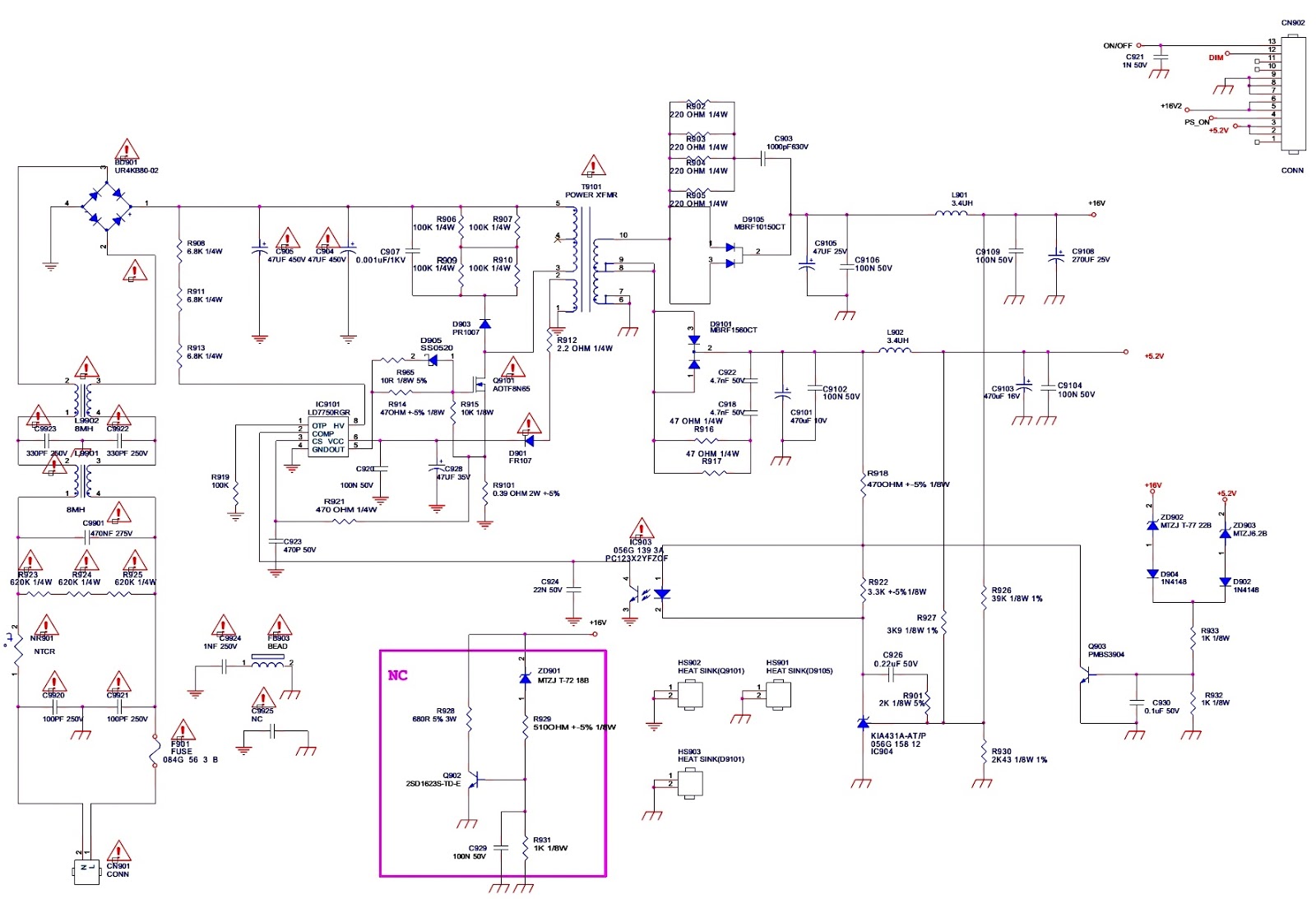
AOC LE22H158 LED TV POWER and LED DRIVER SCHEMATIC

SMPS and LED DRIVER STAGE CIRCUIT - AOC LE22H158 - 22 inch LED TV
SMPS & LED DRIVER SCHEMATIC
CLICK ON THE SCHEMATICS TO ZOOM IN

Thursday, June 25, 2015

TRANSISTORIZED SMPS POWER SUPPLY TROUBLESHOOTING – PART2

Now, let’s come to the COLD side [secondary side] of the SMPS power supply.  Please refer the previous post here for more details.  
The secondary side has the output voltages to main board components.
There are 6 voltage outputs:
+14VDC > to audio output IC.
+5VDC > to CPU side of the syscon chroma IC
An other +5VDC > to tuner stage
+B110VDC > to line output transformer [LOT] section.
+27VDC > to vertical scan output IC
+8VDC > to syscon-chroma IC, pins 17 & 49 of IC8873
Let’s discuss all these supply voltages in detail.
+B110VDC:  this voltage should be there all the time when the set is powered ON; provided there is no fault to primary [HOT] side of the SMPS.
+27VDC:  this voltage too will be there all the time when the set is powered ON; provided there is no fault to primary {HOT] side of the SMPS
+14VDC: this voltage too will be there, when the set is powered ON.
Then comes +5VDC [CPU]:  this voltage is the output from a voltage regulator IC; 78L05.  It too will be, and should be there, as the input to this regulator IC will be present when the set is powered ON.  Refer to the circuit diagram.  Input voltage to this regulator IC comes from pin-14 of the SMPS transformer [after rectification].
The +8VDC 7 +5VDC< {the voltage goes to pin36}are switched type, means these tow voltages will be absent when the set it powered On.  These voltages will be present only after we press either the power button on the remote control handset or at the front pane control of the TV set.  Here more description is needed I thinks.
Take the case of these two voltages only.
Refer the circuit diagram.
Consider all these 3 voltages [+5V CPU, +5VDC, +8VDC]
The source of all these voltages are generated by pin-14 of the SMPS transformer, and then rectified by (D604-FR104).  The rectified voltage is then fed to input of the regulator IC 67L05, which in turn outputs +5VDC CPU.  It will be present all the time, because this voltage is needed to CPU section circuit inside the syscon-chroma IC.  Without this voltage, the CPU section circuit within the IC wont work and there by the set too will not response to any external or remote commands.  In short, the set will be dead.  This voltage is not switched type.  Means it will always be present.  The rectified voltage is also fed to collector of a NPN transistor [V507-C8080] and the collector of another NPN transistor [V508-C8050]; switches the +5VDC.  Refer the circuit diagram and try to understand what happens when we Switch ON the set first, after it is plugged to AC mains, and then we press the power button; either at the remote control, or at the front panel of the TV set.
When we first Switch ON on the set:
+B110VDC is OK - present
+27VDC is OK – present
+5VDC (CPU) is OK – present.
+14VDC is OK – present.
But; there will be no 8VDC & 5VDC. Both these voltages are by-passed by transistors V607 & V508 respectively.
Why?  Here comes the point.
Note the circuit with NPN transistor V507-C8080.
Its base terminal is pulled down to 8.7VDC by using a Zener diode [VD8].  By no means the voltage at this pont will go up, than the break-down voltage of this zener diode; ie 8.7V.
But, from where this voltage comes from?
There is 3.3KOms resistor connected to the cathode of this Zener diode; from the 27VDC voltage output. 
Now what happens?
When we press Power  button either on the remote control or at the front panel  control of the set; to Power On; there should be 8VDC to the base terminals of transistor V507 .  But, it won’t be there now.
Why?
Refer the circuit diagram once again.
  The base of this transistor is connected to [Power On] pin-64 of the syscon IC.  The voltage level of this pin will be hight [=H]; when we switch On the set.  Just see, this high voltage is fed to the base of a NPN transistor [Q210-2SC1815].  The collector voltage to this transistor is fed from (+5V CPU), via a serial resistor CR292, and then a LED (power indicator) and an other resistor R291.
As we know, when the base bias of an NPN transistor is at high [H] level, it will conduct and its collector voltage will drop considerably due to load.  Here the emitter of this transistor is grounded.  So, when its base voltage is high [H], its collector voltage sill be low.
  In fact, when we switch On the set by its AC main Power Switch, the system control section voltages to the IC will be present, the voltage at pin number 64 of IC8873 will be high[H], and the voltage at the collector of Q210 will be low, and in turn the base voltage of +8V regulator transistor too will be low.  So this transistor won’t conduct, and there will be no +8V.
Let it be.
  Now come over to the base of V508; the 5VDC controller transistor C8050.
Refer the circuit diagram again.
 Its collector terminal get voltage from the cathode of D604 itself; through resistors R572 & R571.  The base of this transistor is pulled down to 5V by using a 5V6 zener diode, and the base bias comes from the emitter of V507 [+8VDC].
It is clear that the base bias voltage to this transistor will be present only after the +8VDC has been bypassed by V507.  In short, there will be no +5VDc without +8VDC.
When +8VDC is present, +5VDC too will be there, and should be.
In short; the Main Switching Point to these tow voltages are of pin-64 of the system control IC.
  When the voltage level of this pin is high [H], there will be no +8VDC & +5VDC.  When we press the power button, the voltage at pin-64 of the IC will go low[L], the collector terminal voltage of Q210 will go up; and the base voltage of V507 too.
  Now the transistor V507 will conduct (bypass) +8VDC.  The base bias of V508 will go up and it too will start to bypass the +5VDc.
This is the main switching process takes place, when we press the Power button on the remote control.
Please do not mind my language.  I’m not a person belongs to an English speaking country.  Please try to understand the idea I’ve tried to express.
Any comments? Any suggestions?  Please respond.  I'm here waiting.    google.com/+GopakumarGopalan

Wednesday, June 24, 2015

TRANSISTORZED SMPS POWER SUPPLY TROUBLESHOOTING – PART-1

Set dead. AC fuse blows up instantaneously the set is switched ON.
No DC voltage across C507 [main filter capacitor]
The type of SMPS here in discussion is composed of transistors.  This type of SMPS is used with many brand and models of TVs.  Troubleshooting to this type of SMPS is rather easy than related to STR based ones.  If you get the set for repair in dead condition; isolate the secondary +B voltage [110VDC] from the rest of the circuit by anyway.  This voltage is fed mainly to Horizontals Output and Horizontal drive stages.  Now proceed.
No DC voltage across C507 [main filter capacitor] (100 to 250MFD 450VDC)
See the circuit part.  The AC mains voltage is lead to the rectifier section circuit through a line filter choke L501 and a serial fuse.  This voltage is then rectified and converted to DC voltage, by using 4 rectifier diodes.  If any of these diodes has shorted junction, the AC fuse will blow up as soon as the set is switched ON.  Therefore if you see a blown up fuse; be sure that some short circuited component/s at its main rectifier section circuit or the rectified DC voltage line.
The best way to detect this short circuit is to measure the DC resistance across the main filter capacitor terminals.  It should not show a short circuit.  If it does, de-solder out the SMPS drive transistor and measure it again.  If there is no short circuit detected now,; be sure that the SMPS drive transistor has damaged [collector to emitter leak].  Never replace it, and power up the circuit now.  There shouldbe a reason for this damage to the transistor.  Make sure that there is no damage to other associated component/s with it.  It is best practice to replace the other two small signal transistors with new ones.
De-solder out the other two transistors.  Note their numbers and position in circuit.  One of it is PNP and the other is NPN type.  Now check the other components. Resistors, zener diodes etc:-  Unsolder up one end of each component, and measure its characteristic.  If found OK, solder it in place.  You must be patient and concentrate on work.  Hurry up does not go.
See the circuit.  The rectified DC voltage passes through the primary winding of the SMPS transformer; then to the collector terminal of SMPS drive transistor. As we have already de-soldered out this transistor from circuit, there should not be any short circuit to this votage line to ground now.  If it shows, be sure that the SMPS transformer is damaged [winding short between its primary and secondary].  But this kind of fault is very rare.  Sometimes 0.01% or so.  Can’t say never.  Might be!
Now check the DC resistance across the terminals of the main smoothing capacitor.  It should not measure any short circuit now.  Set the meter to Ohms range, and measure this. Never set it to KOhms range.  Suppose still the meter shows a short circuit.  See; there is no SMPS drive transistor in place.  Then which component/s should be suspected?.  Either the rectifier diodes or the ceraminc capacitors connected in parallel across each of it might cause this.  Check all the four diodes for reverse leak.  If any one among it shows a short circuit, replace all four of it at one time.  It will be the best.
Here one main point to recall is, the rectified DC voltage across the main filter capacitor will be higher than the AC input voltage.  If AC input voltage is 220VAC, this voltage will come around 345VDC or more; and it should be. If not, be sure that the rectifier diodes are faulty.  Replace all these four diodes along with the ceramic capacitors connected in parallel with it. Never forget to check these ceramic capacitors.  They too are likely to be faulty. All of it might be 4.7KPf 630VAC.  If all the components are found OK, plug in to aC power; after inserting a fuse of appropriate specs. 3.5Amps 250VAC.  In rare cases, when we power up the set, with degaussing coil connected, the AC fuse blow up.  If so, the degaussing posistor is short circuited, and should be replaced.
Here we can end with the troubleshooting to primary side of the SMPS circuit.  There is not much more to check with this section. 
Beware:  the primary section circuit will be always HOT, irrespective of connected AC mains phase.  So, take care when you work with this section circuit.  Use of a hand glove is recommended.
Troubleshooting the secondary section circuit will be described by the next post here.
NB: check the resistor and capacitor connected across the primary winding of the SMPS transformer; for open or loose solder terminals. (R525 &C516).  These two components are so critical.  Damage to any one among it will result in the failure (short) of SMPS drive transistor; at the instance of switch ON the set to AC mains.  So, look for any damage or loose solder terminals to these components before power up this circuit.  You won’t get any time to check this fault.  So be cautious.
                                       See the second part for more.

Tuesday, June 23, 2015

TDA8873 SYSCON-CHORMA IC – CIRCUIT TROUBLESHOOTING

Some Faults that can occur due to defects to this IC are:
Power does not switch ON.
TV/AV selection is not possible.
Picture lacks black level.
Tuner does not work.
No EHT.
Horizontal Output Transistor fails frequently.
Audio problems.
Out of synchronized picture.
Displaced picture [horizontally]
Before proceed to troubleshoot, make sure that the SMPS section circuit is woking properly and all the secondary voltages generated are present.  Check the +5VDC & +8VDC.  These two voltages are the supply voltages to TDA8873.  If all these voltages are present, and still the IC do not work, we can assume that the IC is defective.  Check the main supply voltage; 8VDC at pin-17.  The 8VDC is supplied to this pin only.  No other pins receives this voltage.  Check this voltage first.
If it is OK, proceed.
If not, check V507-2SC8080 transistor and associated components at the SMPS section circuit. 
Assuming that this voltage is OK;
Check the voltages at these pins; 3,9,36 & 55.  At all these pins, the voltage should be 5VDC.  If absent, check the 5V voltage regulator IC used at SMPS section, IC607-78L05 & transistor V505-C8050 and related components.
Here one point to note is, with the SMPS circuit used here with this circuit; if there is no 8VDC; the 5VDC too will be absent. 
Assuming that all the voltages stated above are Ok; but the IC do not function:
If so; the first check should be concentrated toward the soldering terminals of the IC.  There are 64 pins.  If any of these pins have loose solder, erratic symptoms will be the result.  So; first make sure that these solder terminals are OK; and have no dry solder points.  Normally it will be too difficult to detect a dry solder terminal, as it will be too microscopic for normal vision.  So it will be the best practice to re-solder all these 64 pins; by applying a little more fresh solder to each terminals, without making any solder-bridge short in between adjacent terminals.  Be sure not to apply too much heat for long time, at these termilas, as it might damage the IC.  The soldering should be done as fast as possible; and should be clean.
Now check all the other pin voltages. 
Measure the voltages at SCL & SDA [Serial Clock & Serial Data] pins; 58 & 57 respectively.  Both of this should be around 2.8VDC.  if any of these voltages are either too low or high; the IC is defective.
No repair.  Replacement is the only remedy.
Next check the Power-ON signal voltage present at pin 64.  When you press the Power On button on the remote control, this voltage should be vary to High/Low [4.8VDC.0.5VDc.]
If not; the IC is defective. The system control section inside it does not work properly.
Check the voltage at pin-5.  This is the Reset voltage to IC and should come around 3.2VDC.  if absent; check Q203-A1015 and Zener diode VD201, connected to its base terminal.
Assuming that all the above voltages are normal:
Measure the voltage at pin-13 [horizontal out signal].  It should be about 0.4 to 0.7VDC.  will have an oscillating frequency of ~ 15.625KHz.  if your meter is capable of measuring frequency; you can measure this frequency directly from this point. If this frequency and the voltage at these terminals is abnormal, the IC is defective.
In most cases; measuring the voltages said above will reveal the condition of this IC; whether defective or good.
Click on the schematic to zoom in

Saturday, June 20, 2015

AKAI 14CRM – TROUBLESHOOTING – From My SERVICE TABLE TODAY

Troubleshooting – Akai 14CRM, 14 inch color TV.  No picture – raster OK – no system Functions
The set switches ON, firmware loads properly, raster appears, suddenly goes to AV mode, displaying AV on the screen.  After few seconds, this AV display too will be out, and the set is irresponsive to any external commands, either by remote control or by the front control panel switches.
Powered OFF the set, unplugged it from AC mains, and re-plugged it back to AC, to check whether a hard reset will help.  No effect.  The same thing as before has happened.
IC used as system control-chroma jungle is TDA11105/PS/V3/3/AT2
System memory IC used is 24C16WP
The above mentioned symptom mainly indicates the main system control memory IC fault.  I’ve came across this type of problem, at about 6 months back, with a Panasonic 24 inch CTV.  Here I did recall it.
Anyway; I’ve to confirm the fault before replace the memory IC.  Checked the main supply voltage to 24C16.  OK. 5VDC is there.
Checked the Serial Data and Serial Clock [SCL SDA] signal voltages.  Found fine.  Shows 2.7VDC to each of these two pins.
Checked the voltage to control panel switch board.  OK.  4.87VDC.
Checked all the micro switches for its contact continuity.  3 out of the 6 of it have bad contacts detected.
Replaced all the 6 micros switches to make sure that they are OK.
Now I tried to control the set by the front panel switches.  Do not control.
Checked all the pin voltages of TDA11105; with reference to the schematic diagram.  All the voltages were found normal.
Fault to main system control memory IC 24C16WP confirmed.
Replaced it with a new one.
OK.
There was no other problem detected.
Re-tuned the set to On-Air transmission.  Fine.  Auto-search tuning is ok.  Set auto tunes, locks the channels in programs.

Friday, June 19, 2015

LG LPC-LM530A MP3 - CD CASSETTE – Circuit Diagram

SCHEMATIC DIAGRAM - LG LPC LM530
Used ICs: AN22004A – MN6627933CG – M12L16161A – LC877480 – TDA7468 – LA4663 – KIA6289 – BA3126
Power consumption > 30W
Mass > 2.75kg
External dimensions > (W x H x D) 550 x 290 x 220mm
Output Power > 7.5W x 2
Speakers > 8Ω x 2
Battery Operation DC 12V, eight “D”(R20) batteries (not supplied)
Frequency response > 100 ~18000Hz
Signal-to-noise ratio >59dB T.H.D 0.7%
Tuning Range > 65~74MHz, 87.5~108MHz or 87.5 ~108MHz
Intermediate Frequency > 10.7MHz
Antenna > Telescopic antenna
Tuning Range > 522~1611kHz or 530 ~1610kHz
Intermediate Frequency > 450kHz
Antenna Ferrite bar antenna
Recording System > 4 Tracks 2 channel stereo
Frequency Response > 125 ~8000Hz
Signal to Noise Ratio > 40/45dB (REC/PLAY)
CDP
CONTROL PANEL
TAPE DECK
POWER AMPLIFIER & EQUALIZER
EXPLODED
PWB

LG XC62 LGXCS62F – MINI STEREO SYSTEM – HOW TO RESET – EXPLODED VIEW – Troubleshooting Chart

LG XCS62F - HOW TO RESET - HOW TO DISASSEMBLE
AMPLIFIER
Output Power 30W + 30W
T.H.D 0.5%
Frequency Response 40 ~ 20000Hz
Signal-to-noise ratio 75db
SPEAKERS
Type 1Way 1Speaker
Impedance 4Ω
Frequency Response 75 ~ 17000Hz
Sound Pressure Level 83dB/W (1m)
Rated Input Power 30W
Max. Input Power 60W
Net Dimensions (WxHxD) 144 x 243 x 171mm
Net Weight (1EA) 1.47kg
HOW TO RESET
You can reset your unit to initial status if malfunction occur(button malfunction, display, etc.).
Using a pointed good conductor (such as driver), simply short the RESET jump wire on the inside of the volume knob for more than 3 seconds.
If you reset your unit, you must reenter all its settings (stations, clock, timer)
1. To operate the RESET jump wire, pull the volume rotary knob and release it.
2. If you wish to operate the RESET jump wire, it is necessary to unplug the power cord.
EXPLODED VIEWS
CD MECHANISM
TAPE DECK MECHANISM
SPEAKER BOX
TROUBLESHOOTING CHARTS
FLD DISPLAY
SMPS
MICOM PART
POWER AMPLIFIER
CLICK ON THE PICTURES TO MAGNIFY
                See the Schematics (Circuit Diagram)

Thursday, June 18, 2015

HP pavilion ZE1000 HOW TO REMOVE KEYBOARD – OPTICAL DRIVE – HARD DISK

Keyboard_SDRAM_Hard disk drive & Optical drive removal – Hp pavilion ZE1000 series notebook PCs.
To remove the keyboard and optical drive, proceed the following order:
Battery => Lion 8-cell > F3410-60911
Drive, hard disk [20MB, 9.5mm, IBM (Diablo) ATA100  > 0950-4163
SDRAM, 128mb, PC133 SODIMM(x16) > 1818-8504
SDRAM, 256mb, PC133 SODIMM(X16) > 1818-8635
KEYBOARD > F3420-60913
DVD > F3410-60917
DVD,CD-RW > F3410-60919
BATTERY REMOVAL PROCEDURE
Slide the battery’s release latch, and then pull the battery out of its compartment.
HARD DISK DRIVE
Remove both hard drive retaining screws from the bottom of the notebook.  Carefully remove the hard drive from of the notebook.
Remove all four screws from the tray and drive case, and then remove the drive from the tray.
(If you’re installing a new hard disk drive, install the factory software and O/S on the drive before loading any additional software.)
The notebook has no SDRAM built into its motherboard, but has two slots for removable SDRAM modules in a compartment on the bottom of the unit. (One of these slots contains a module installed at the factory). You can use these slots to expand your unit’s RAM. Use HP PC133 SDRAM modules only, or your notebook will not boot up.
Turn off the notebook: click Start, Turn Off Computer, Turn Off.
Unplug the AC adapter (if present) and remove the notebook’s battery.
On the bottom of the notebook, loosen the screw holding the RAM cover (the cover retains the screw), and remove the cover.
Release the two latches at the sides of the SDRAM module by pushing them gently outward  (away from the sides of the module). When you release the latches, the free edge of the module pops up.
KEYBOARD REMOVAL
Unplug the AC adapter, if present, and remove the battery.
Use the flat-blade screwdriver to carefully pry up the right end of the keyboard cover, just above the Delete key, then lift the cover off of the notebook.
Insert the tabs on the left end of the cover into the slots in the notebook’s case, and then gently press along the length of the cover to snap it into place.
Remove both retaining screws from the top of the keyboard.
Raise the top of the keyboard, then lift the keyboard up and out of the notebook, and lay it face down on the top case, forward of its normal position.
OPTICAL DRIVE REMOVAL
Remove both retaining screws from the back of the optical drive. 5. Carefully slide the optical drive out of the notebook.