Thursday, June 16, 2016

How to enter service mode – LG CM9730 – Software update – Exploded view

HIDDEN KEY MODE
Push both Front key and RCU key to activate it for 5 seconds.
1. Disc Lock On/Off (CD Function Only Active)
Front Key : STOP
RCU Key : STOP
2. Check Version and Option code
Front Key : STOP
RCU Key : PLAY/PAUSE
You can change [Audio MCU Version <=> CD Controller Version <=> EEPROM Option] by SKIP [+/-].
3. Clear EEPROM
Front Key : STOP
RCU Key : SKIP-
4. Edit EEPROM
Front Key : STOP
RCU Key : SKIP+
You can change the digit option by SKIP +/-.
You can edit 0~f by REPEAT or PLAY/PAUSE key.
5. Bluetooth DUT
Front Key : STOP
RCU Key : PROGRAM
Bluetooth model only
6. Power Disc Lock On/Off (CD Function Only Active)
Front Key : STOP
RCU Key : EQ
7. Amp Clip On/Off
Front Key : STOP
RCU Key : Mute
Amp Clip Mode Change (Amp Clip On --> Amp Clip Off --> Level Down display)
8. Demo ALL Key Lock (CM9520/CM8520 Only)
Front Key : STOP
RCU Key : 9
Demo All Key Lock Change (All Key Lock On --> All Key Lock Off)
> Working on Demo Operation only
> When All Key Lock, Volume Key work only
> After All Key Lock Off, it can unlock Demo Mode.
Exploded View [Click on the pictures to zoom in]
PROGRAM UPGRADE
1. Check the download file name.
[File Name Micom:CM9730_”version”.  Mpeg: HEX HE004_”version”.BIN EQ:EQ_PRG.BIN]
There is the Update File only in the USB storage.
2. Copy the download file to the USB storage.
3. Insert the USB storage on USB1 or USB2 Function.
4. VFD Display
1) MICOM : “WRITE XX”
2) Mpeg : “FIRMWARE”
3) EQ : “EQ DOWN”
5. Complete Update
1) When the Set is turned off automatically after display "UPDATED", remove the USB storage.
2) Unplugged the power cord after display "FINISHED", then remove the USB storage.
Upgrade required time
Upgrade required time is determined depending on the Writing time considering the Download stability.
[Upgrade time. MICOM: about 60sec. Mpeg: about 15sec. Eq: about 5sec]

Wednesday, June 15, 2016

CM9730 LG SUPER POWER MINI HI-FI SYSTEM - troubleshooting

NO POWER
If the unit doesn’t work by no power problem, repair the set according to the following guide.
FUSE / BRIDGE DIODE / THERMISTOR
Check and replace F901, BD901, TH900, TH901, TH902 on SMPS board.
1) Check if the fuse F901 is open or short-circuit.
2) Check if the bridge diode BD901 is short-circuit by over current with a digital multi meter.
3) Check if the NTC thermistor TH900 ~ TH902 is normal or open.
NO POWER
If the unit doesn’t work by no ±PVDD problem, repair the set according to the following guide.
NO AMP POWER
Check and replace F911, Q911 ~ Q914 on SMPS board.
1) Check if the fuse F901 is open or short-circuit.
2) Check the Drain-Source or Drain-Gate, Gate-Source Resistance of Q911~Q914 with a digital multi-meter.
If it is short condition, it’s destroyed. Replace it with a new one.
(Replace 4 FET at the same time although several FET is OK)
NO BOOTING WHEN POWER ON THE SET
The set doesn’t work when presses the power button on the front board or the remote control.
FLASH MEMORY (IC101)
Check and replace IC101 on MAIN board.
1) Check the 5.6 VA (CN102) and 3.7 VA (IC104) in standby mode.
If there is no 5.6 VA, check the SMPS and if doesn’t appear 3.7 VA, check IC104.
2) Check 5.6 VA, 12 V, FL+, FL-, an 32 V when power on the set.
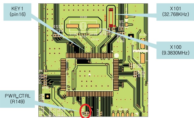
- If the set doesn’t work regardless of what the KEY2 changes high to low while pressing the power button.
X100 and X101 work normally but, if you cannot power on the set, replace the IC101 with a new one on the MAIN board.
VFD IS NOT DISPLAYED WHEN POWER ON THE SET
When power on the set, any icons or characters on VFD are not displayed.
VFD (DIG301)
Check and replace DIG301 on FRONT board.
1) Check if 32 V, FL+ and FL- are output from SMPS to VFD via the MAIN board.
2) Check if the IC101 outputs VFD_RST, VFD_CLK, VFD_STB and VFD_STB to the FRONT board.
3) Check if the VFD grid current amplifier circuit (Q301, Q303, Q304) on the FRONT board.
Check the drive signal to the transistor’s base.
If the control signals from VFD (TP302, TP303, TP304) isn’t output, replace VFD with a new one.
If the transistor doesn’t work, replace it.
NO BOOTING IN CD/USB FUNCTION
After you turn on power key and displayed message in the following order
(HELLO > VOL XX > CD or USB) on VFD,
it will not display other message on VFD, and it will not boot-up normally.
NO VCC33, VCC12
Check and replace IC505, IC509 on MAIN board.
1) Check Voltage of IC505 pin2 on MAIN board.
If IC505 pin2 (about 4.9 V) & D501 Input 5.6 VA doesn’t come out, check 5.6 VA from SMPS board.
2) If IC505 pin2 (about 4.9 V) is normal, check the PWR_CTRL (IC505 pin1) is high (about 3.3 V).
If PWR_CTRL isn’t high, check pin63 of IC101 & R149,R503.
3) If PWR_CTRL is high, check R592, R593 and if there’s no defective component then replace IC505.
4) If 3.3 V (VCC33) is normal, check output (pin2, 4) voltage of IC509.
If 1.2 V of IC509 pin2, 4 doesn’t come out, then replace IC509.
NO BOOTING IN CD/USB FUNCTION
After you turn on power key and displayed message in the following order
(HELLO > VOL XX > CD or USB) on VFD,
it will not display other message on VFD, and it will not boot-up normally.
CRYSTAL (X501)
Check and replace X501 on MAIN board.
1) If 3.3 V & 1.2 V is normal, check Reset ‘High’ of IC501 pin153 on MAIN board.
If MAIN_RESET isn’t high, check MICOM (IC101) pin59.
2) If MAIN_RESET is high, check the soldering status of 12 MHz crystal (X501).
3) If the crystal (X501) doesn’t oscillate, check R541,R542,C517,C518 around crystal (X501).
If there’s no defective component, then replace X501.
NO BOOTING IN CD/USB FUNCTION
After you turn on power key and displayed message in the following order
(HELLO > VOL XX > CD or USB) on VFD,
it will not display other message on VFD, and it will not boot-up normally.
SERIAL FLASH (IC503)
Check and replace IC503 on MAIN board.
1) If the crystal (X501) does oscillate, check serial flash (IC503) on MAIN board.
Check pin8(VCC), pin6(CLK), pin1(CS#), pin2(DO), pin5(DI) of below waveform.
2) If pin1, 2, 5, 6, 8 doesn’t come out, check damping resistor (R511, R513, R514, R515) of IC503.
If damping resistor of IC503 is OK, then replace IC503. (it need to download program)
3) After change IC503, if It is still not below waveform, check IC501(DSP IC).
NO BOOTING IN CD/USB FUNCTION
After you turn on power key and displayed message in the following order
(HELLO > VOL XX > CD or USB) on VFD,
it will not display other message on VFD, and it will not boot-up normally.
 SDRAM (IC502)
Check and replace IC502 on MAIN board.
1) Check below waveform & soldering status of SDRAM (IC502) on MAIN board.
If pin17(#CAS), pin18(#RAS), pin19($CS), pin38(CLK), pin29(address), pin2(DQ) doesn’t come out,
check damping resistor (R508, R506, R504, R507).
2) If resistor is OK, then replace IC502 (SDRAM).
3) After change IC502, if It is still not below waveform, check IC501 (DSP IC).
NO BOOTING IN CD/USB FUNCTION
After you turn on power key and displayed message in the following order
(HELLO > VOL XX > CD or USB) on VFD,
it will not display other message on VFD, and it will not boot-up normally.
DSP IC (IC501: MLC3700A)
Please check and replace IC501 on MAIN board.
1)After check them by previous pages about NO Booting, if the set is still no booting,
Check soldering status of IC501.
Check boot strap option (R598, R594, R597) of IC501(DSP IC).
2) If below bootstrap waveform doesn’t come out, then replace IC501 (DSP IC).
NO OPERATION OF MD
When no sound output in the CD function, you cannot listen to music reading data from a CD disc if the servo motors in MD don’t work. This step is for checking the
SPINDLE MOTOR among them.
Check and replace IC407, IC408 on MAIN board.
1) Check the SPDO signal from Pin16 of IC407.
If no signal, check 3.3 V(RF) and X402.
2) Check the SP- & SP+ from IC408 to CN405 for driving SPINDLE motor. It is about 3.6 Vp-p.
If no signal, check +1.8 V and +5 V for IC408.
3) Check if the FFC cable is solidly connected between CN405 and MD.
4) Check the MD.
If the spindle motor is sort-circuit or has any trouble, it can not rotate CD discs.
Please check the function after changing another MD.
NO OPERATION OF MD
When no sound output in the CD function, you cannot listen to music reading data from a CD disc if the servo motors in MD don’t work. This step is for checking the
SLED MOTOR among them.
Check and replace IC407, IC408 on MAIN board.
1) Check the SLDO signal from Pin15 of IC407.
If no signal, check 3.3 V(RF) and X402.
2) Check the SLED+ & SLED- from IC408 to CN405 for driving SPINDLE motor. It is about 2.9 Vp-p.
If no signal, check +1.8 V and +5 V for IC408.
3) Check if the FFC cable is solidly connected between CN405 and MD.
4) Check the MD.
If the sled motor is sort-circuit or has any trouble, it can not move the pick-up module.
Check the function after changing another MD.
NO OPERATION OF MD
When no sound output in the CD function, you cannot listen to music reading data from a CD disc if the servo motors in MD don’t work. This step is for checking the
TRAY OPEN/CLOSE MOTOR among them.
Check and replace IC407, IC408 on MAIN board.
1) Check MOT_OPEN & MOT_CLOSE signals from Pin62 & 63 of IC501 to IC408.
If no signal, check +1.8 V & + 5 V to IC408.
2) Check LOAD± from IC408 to CN405 for driving the tray open / close motor. It is about 3.85 Vp-p.
If no signal, check +5 V to IC408. If it has any trouble, replace it with a new one.
3) Check if the FFC cable is solidly connected between CN405 and MD.
4) Check the MD.
If the tray motor is sort-circuit or has any trouble, it can not open or close the tray.
Check the function after changing another MD.
NO OPERATION OF MD
When no sound output in the CD function, you cannot listen to music reading data from a CD disc if the pickup module in MD doesn’t work. This step is for checking the LASER TRACKING ACTUATOR.
Check and replace IC407, IC408 on MAIN board.
The tracking actuator makes the laser beam be positioned in the center of a track on CD disc.
1) Check the TRD signal from Pin14 of IC407.
If no signal, check 3.3 V(RF) and X402.
2) Check T- & T+ from IC408 to CN404 for driving the tracking actuator.
If no signal, check +1.8 V and +5 V for IC408.
3) Check if the FFC cable is solidly connected between CN404 and MD.
4) Check the MD.
If the pick-up module has any trouble, it cannot move the laser beam on the left or right side.
Check the function after changing another MD.
NO OPERATION OF MD
When no sound output in the CD function, you can not listen to music reading data from a CD disc if the pickup module in MD doesn’t work. This step is for checking the
LASER FOCUSING ACTUATOR.
Check and replace IC407, IC408 on MAIN board.
How to troubleshoot
The focusing actuator makes the laser beam keep a regular interval with the surface of a CD disc.
1) Check the FOD signal from Pin13 of IC407.
If no signal, check 3.3 V(RF) and X402.
2) Check F- & F+ from IC408 to CN404 for driving the focusing actuator.
If no signal, check +1.8 V and +5 V for IC408.
3) Check if the FFC cable is solidly connected between CN404 and MD.
4) Check the MD.
If the pick-up module has any trouble, it can not move the laser beam on the top or bottom side.
Check the function after changing another MD.
NO SOUND
There is no sound output in the CD FUNCTION, repair the set according to the following guide.
Check and replace IC501, IC600 on MAIN board.
1) Check CD_BCK, CD_LRCK, & CD_DATA signals from IC407 to IC501.
If no signal, check if the RF & servo signals from MD is entered to IC407.
Refer to the “No operation of MD” guide.
2) Check the following I2S signal flow. < I2S audio signal Interface >
- DAC_BCK : IC501_pin4 > IC600_pin4
- DAC_LRCK : IC501_pin5 > IC600_pin5 (44.1 kHz)
- DAC_DATA : IC501_pin85 > IC600_pin6, 9
- DAC_MCLK : IC501_pin3 > IC501_pin82
If there is any trouble, check the power for each IC. The power is normal but, if the signal waveform to the IC is distorted or no signal, replace it with a new one.
3) Check if “Digital audio AMP block”.
NO SOUND
There is no sound output in the USB FUNCTION, repair the set according to the following guide.
Check and replace IC501, IC504 on MAIN board & IC3U01 on USB board.
How to troubleshoot
1) Check +5VU to USB board.
If +5.6 VA to pin2 of IC3U01(LDO) doesn’t come out, check pin4, 5 of CN502.
If +5.6 VA is normal & +5VU of IC3U01 pin3 doesn’t come out, and then replace IC3U01.
2) Check USB D± from main board to USB board.
a. Check USB_HUB_DN/DP signals to IC501(pin16, 18)
b. Check USB1/2_DN/DP signals from IC501 to CN502 (pin1, 2, 9 & 10)
If there is any trouble, check the power for each IC. The power is normal but, if the signal waveform to
the IC is distorted or no signal, replace it with a new one.
3) Check if “Digital audio AMP block”.
NO SOUND
There is no sound output in the AUX FUNCTION, repair the set according to the following guide.
Check and replace IC202 on MAIN board.
How to troubleshoot
1) Check AUX_L/R signals to IC202 (Pin7, 8).
2) Check if DAC_BCLK, DAC_LRCLK, & DAC_MCLK are entered from IC501 to IC202.
3) Check if ADC_DATA is entered from IC202 to IC501.
If no signal, check +5 V & +3.3 V(ADC) for IC202. If is NG, replace it a new one.
4) Check the following I2S signal flow from IC501 to IC600. (Refer to Item 6-1.)
If there is any trouble, check the power for each IC. The power is normal but, if the signal waveform to
the IC is distorted or no signal, replace it with a new one.
5) Check if the digital audio AMP block is okay. Refer to “Digital Audio AMP” guide.
If AMP is damaged, replace it with a new one.
NO SOUND
There is no sound output in the PORT. IN FUNCTION, repair the set according to the following guide.
Check and replace IC202 on MAIN board.
How to troubleshoot
1) Check PT_L/R signal from JOG board to MAIN board.
2) Check if PT_LR is entered Pin4 & 5 of CN3J01 Ö Pin4 & 5 of CN3V02 Ö Pin21 & 20 of CN3V01.
3) Check POT_L/R signals to IC202(Pin21, 22).
4) Check if ADC_BCK, ADC_LRCK, & DAC_MCLK are entered from IC501 to IC202.
5) Check if ADC_DATA is entered from IC202 to IC501.
If no signal, check +5 V & +3.3 V(ADC) for IC202. If is NG, replace it a new one.
6) Check the following I2S signal flow from IC501 to IC600. (Refer to Item 6-1.)
If there is any trouble, check the power for each IC. The power is normal but ,
if the signal waveform to the IC is distorted or no signal, replace it with a new one.
7) Check if the digital audio AMP block is okay. Refer to “Digital Audio AMP” guide.
If AMP is damaged, replace it with a new one.
NO SOUND
There is no sound output in the TUNER FUNCTION, repair the set according to the following guide.
Check and replace IC202, TU801 on MAIN board.
1) Check if TUNER_LR is entered from Pin1 & 3 of TU801 to IC202(Pin23, 24).
If no signals, Check +3.3 V for Tuner power.
Check if the Tuner control signals (CLK, DAT, CE, RST, GPO2) are entered from IC101 to TU801.
If it doesn’t work, replace TUNER with a new one.
2) Check if ADC_BCK, ADC_LRCK, & DAC_MCLK are entered from IC501 to IC202.
3) Check if ADC_DATA is entered from IC202 to IC501.
If no signal, check +5 V & +3.3 V(ADC) for IC202. If is NG, replace it a new one.
4) Check the following I2S audio signal flow from IC501 to IC600. (Refer to Item 6-1.)
If there is any trouble, check the power for each IC. The power is normal but, if the signal waveform to
the IC is distorted or no signal, replace it with a new one.
5) Check if the digital audio AMP block is okay. Refer to “Digital Audio AMP” guide.
If AMP is damaged, replace it with a new one.
NO SOUND
There is no sound output in the MIC IN FUNCTION, repair the set according to the following guide.
Check and replace IC508, IC506 on MAIN board.
How to troubleshoot
1) Check MIC_SIG signal to Pin6 of CN506.
If no signal, Check the signal to Pin6 of CN3M01 on the MIC board.
Check if the signal is entered from Pin6 of CN3M01 to MAIN board.
2) Check if MIC_SIG is entered from Pin6 of CN506 to Pin3 of IC506 (MIC AMP).
3) Check if the amplified signal is entered from Pin4 of IC506.
If no signal output, check +12 V for IC506, replace IC506 with a new one if it has a problem.
4) Check if MIC_BCK, MIC_MLCK & MIC_LRCK is entered from IC501 to IC508.
Check if MIC_DATA is entered from Pin9 of IC508 to Pin7 of IC600.
If no signal, check +5 V & +3.3 V for IC508. If it is abnormal, change replace it a new one.
5) Check the following I2S signal flow from IC508 to IC600.
If there is any trouble; check the power for each IC. If the signals are abnormal, replace it a new one.
6) Check if the digital audio AMP block is okay. Refer to “Digital Audio AMP” guide.
If AMP is damaged, replace it with a new one.
NO SOUND
There is no sound output in the BLUETOOTH FUNCTION, repair the set according to the following guide.
Check and replace IC501 on MAIN board and Bluetooth module on front panel.
How to troubleshoot
1) Check BT_RX, BT_TX signal to Pin5, 7 of CN504.
If no signal, check the signal to Pin5, 7 and Pin1(+3.3 V) of on the Bluetooth module and cable connection state.
If there are no signal out from module, replace new module.
2) Check if BT_RX/TX is entered from Pin5, 7 of CN504 to Pin169, 170 to IC501 (DSP).
3) Check if MIC_BCK, MIC_MLCK & MIC_O_DATA is entered from IC501 to IC600.
If no signal, check VCC12(+1.2 V) for IC501. If it is abnormal, change replace it a new one.
4) Check the following I2S signal flow from IC501 to IC600.
If there is any trouble, check the power for each IC. If the signals are abnormal, replace it a new one.
5) Check if the digital audio AMP block is okay. Refer to “Digital Audio AMP” guide.
If AMP is damaged, replace it with a new one.
AUDIO OUTPUT IS SMALL OR NO AUDIO OUTPUT
Audio signal output is small or not. when you power on the Middle Power Mini System.
Check and replace IC700 ~ IC706 & IC708 on MAIN board.
How to troubleshoot
1) Please check if this system is on bass blast mode.
RL and RR make sound only on bass blast mode.
2) Check the IC700 ~ IC706 & IC708 on your eyes.
3) Check the audio signal output check (Pin13 of IC700 ~ IC706 & IC708).
First, check the PWM Data input (Pin3 pin of IC700 ~ IC706 & IC708).
4) If the audio signal output has no output, try to change IC which has no output.
5) Lastly, check Speaker Terminal (CN702, CN703)
NO POWER ON (STANDBY LED IS BLINKING)
Check and replace Q700 ~ Q705, Q708, Q709, Q714, Q716, Q719 ~ Q724 on MAIN board.
 How to troubleshoot
1) This symptom occurs, when DC protection is detected. Main reasons are like below.
When Some of AMP FETs dead.
Notice for FET service
 In case of RF6775, Metal case, FET Drain, has electric potential. So be careful when you deal with it.
You can see FET after removing heatsink.
Notice for Service
Before repair Main Assy, you need to discharge SMPS.
After then, open the connector.
You should try to change both of +/- FET and Driver IC as a pair.
SPEAKER NO AUDIO
AMP IC:
Check and replace the component on MAIN board.
How to troubleshoot
1) Check supply voltage of AMP(CN700, CN701) & PWM signal
Normal Supply voltage and signal.  Check AMP IC.
Poor supply voltage Ö Check SMPS Assy.
Poor signal. Check PWM IC.
2) Check CSD of FET driver IC (IRS2092 : EAN60778301).
CSD has about 5 V on normal state.  When AMP has problem, CSD is LOW state or keep change LOW to HIGH.

LG CM9730 – SMPS and Main Amplifier – Circuit Diagram - SUPER POWER MINI HI-FI SYSTEM

AMPLIFIER
Output 575 W x 4 (8 Ω at 1 kHz, THD 25 %)
FRONT SPEAKER
Type Low channel 1 Way 1 speaker
High channel 2 way 2 speaker
Impedance 8 Ω
Rated Input Power 575 W
Max. Input power 1150 W
Net Dimensions (W x H x D) 520 x 720 x 499 mm
Net Weight 35.5 kg
SMPS (Power supply regulator) schematic
SMPS - PWB
Power Amplifier and DSP
Click on the schematics to magnify

Tuesday, June 14, 2016

Microlab AH500 HTS - Circuit Diagram - CD4052 – M62446 – 4558 – LM3886 – 2SC5200-2SA1943 Sub-Woofer Output transistor pair

Microlab Home Theater System AH500 - Schematic_ Used Semiconductors: CD4052 – M62446 – 4558 – LM3886 – 2SC5200-2SA1943 Sub-Woofer Output transistor pair
 LED Schematic
Front
Power
Click on the circuit diagrams to magnify

Monday, June 13, 2016

Daewoo-Sony VX 14A1 – VX14AW1 – VX21AW1 – Circuit Diagram – TV-VCR combo: Service Mode - STR F6626 - SMPS - working principle

 Used ICs: STR-F6626 – LA78041 – 24LC08B – LA71076AM – LA76834 – TDA7442 – MM1053 - TDA7267:  Working Principle of SMPS power Regulator Circuit, using STR F6626
Features of the model
1) Chip for TV / video are all 1-Chip.
2) Light / NO adopt the deck of CONNECTOR.
3) Easy to adjustment in the non-adjustment or the remote control.
4) during the operation of the protector circuit, displayed on the LED (vertical protector service during the on / off possible).
5) It can operate without deck.
6) Can service only in the user remote control.
SMPS and Deflection PWB and Circuit Diagram
SMPS Working
Power supply unit Operation (STR-F6626-related)
Vin terminal
START circuit detects the Vin terminal voltage, a circuit for performing the operation start and stop control the IC.
Initial AC power input, and by the condenser (C810) starting resistance of control outside the IC (R806), rising Vin terminal until the operation start voltage (14V)  from the control circuit in the IC to work.  After the control circuit operation, the Vin terminal by TURN ratio wrapped in proportion to the secondary side B + join a stable BACK UP power.  When the B + power on the secondary side drops to about 1/10 than normal (11V), 1 order of Vin fall even in the same proportion UVLO (Under Voltage Lock Out) is to operate . Then, joined by Vin through the start-up resistance again, this voltage is operates in the same manner as the first and leading to 16V.
Oscillator and OCP / FB pin 1
Oscillator of the internal control IC is the reference voltage input terminal is OFF.
IC will start operation by the internal oscillator and Vin voltage reaches the operation start voltage (14V). Internal oscillator, when the charging voltage of the internal C1 is 3.7V
OSC is turned ON, the voltage of C1 is increased to 6.5V.
When the internal oscillator to oscillate MOSFET can Vocp turns ON. This voltage is led OCP / FB terminal, internal OCP / FB COMP voltage
There MOSFET is turned OFF when it comes to 0.73V.
Voltage of C1 is maintained at 6.5V when ON of the MOSFET, to gradually discharge and turned OFF. Discharge time is determined by an internal RC, 50uS
When the discharge to become 3.7V MOSFET is turned ON, IC performs the basic operation by repeating this kind of behavior.
Over-current protection circuit (OCP = Over Current Protector)
OCP circuit operates in PULSE BY PULSE system detects the DRAIN current directly.  Circuit is constituted by COMPARATOR as in Figure 2. Detection voltage Yes is set to -1.37V with respect to the GND of the internal control IC.  No more voltage is turned OFF the internal oscillation operation and participate.
LATCH function  OVP = Over Voltage Protector
OVP (overvoltage protection) circuit and TSD (overheat protection) circuit during operation, a circuit for stopping the operation of the power supply circuit to maintain the output of the oscillator to OFF.
If the operation of the OVP and TSD persists more than 8uS to prevent malfunction due to noise, it is set to work.  When the LATCH circuit operates, Vin voltage of the IC drops to sharply stops operation voltage. Motion also internal constant-voltage circuit is followed by the LATCH circuit operates.  The other hand to work, is because the Vin voltage is not applied to continue.
When the Vin voltage drops to less than the operation stop voltage, IC is asked to supply the Vin through the start-up resistor for the restart, to 16V of operation start voltage reach and, Vin is rapidly decreases with increasing again circuit current. In this case, Vin repeats the UVLO, IC does not operate.
After the order to release the LATCH state, but it should go up from down Vin until less than 6.5V, in general turn off the AC INPUT, comeback It must be dynamic. (Refer the above given circuit)
Click on the pictures to zoom in
Circuit Diagram (Syscon - Tuner VIF and Chroma) & PWB
How to enter and the attitude to the service mode
User remocon sequentially enter in the button input of.
"Menu" => "10" => "11" => "Volume (+ or ) within 3 seconds.
Currently, the term that has been selected is displayed in red, it can move to the adjustment in the direction button. At the time of the service mode is canceled
Press and hold until exiting the "menu" key.
Or press the "Power" key. ( after the adjustment, the memory of the Data is separately required)

Saturday, June 11, 2016

ONIDA 21BLACK FGL - 20XS - How to enter Service Mode – Adjustments

Service Mode 3G(UE-DLX)
The following display comes on the screen by pressing DISPLAY key and VSM key at the same time.
FACTORY
SERVICE MODE
Press CURSOR UP OR DOWN key to be in Service menu.
To select Service Menu parameters use CURSOR UP OR DOWN key and to adjust these parameters use CURSOR LEFT OR RIGHT key.
H-LINE
1) To get H-line press VSM and DISPLAY Simultaneously.
2) Press CURSOR UP KEY to get R CUTOFF.
3) Press '0' to get H-line.
4) To come out of H-line again press '0'
VSM PRESET
There are FOUR VSM
PRESETS.(CARTOON,FILM/POP,NEWS,)
For the setting of individual VSM PRESETS
1. Press VSM and DISPLAY at the same time.
2. Press CURSOR DOWN key to get the Setting for the VSM PRESET.
3. Press CURSOR DOWN key for the selection of each parameter.
4. Use CURSOR LEFT/RIGHT key for their setting as per the table given below.
5. Press VSM Key for selection of VSM PRESETS.
Adjustment Procedure
1) Switch ON the TV Set.
2) Select colour bar pattern {carrier frequency of 38.9MHz} from pattern generator.
3) Connect this signal to the input of Saw Filter(after disconnecting IF output of Tuner)
4) Connect Digital Multimeter to AFC out(pin no. 2 of VCD IC52771, IC201)
5) Adjust VCO coil in such a way that Digital Multimeter shows 4V(sudden change in voltage reading from 8V)
This voltage should be adjusted whenever there is sudden fall from 8V to 1V as shown
NOTE
# use non-metallic adjustment tool (eg~ceramic) for adjustment.
# Correct AFT voltage alignment can be confirmed by monitoring proper waveform at pin no. 38 of VCDIC 52771 IC no. 201./CRO can be also connected to Video OUT terminal.
Low light Adjustment 3G(UE-DLX)
1) Receive the monoscope pattern signal .
2) Select either R CUTOFF , G CUTOFF B CUTOFF in the Service menu.
4) Push 0 key on any mode to make a horizontal line.
5) Turn the screen knob (the Bottom of FBT) gradually from fully left to the right & search for the first appearing colour.
6) Adjust two colours except for the first colour which appears by the adjustment 5) to the white colour with the following 1~ 6 key.
7) Turn the screen knob so that a horizontal line appear slightly.
8) Change the normal screen by pushing 0 key again.
9) Receive the pedestal pattern signal
10) Readjust the Colour of the pattern to white colour by varying 1~ 6
High light Adjustment  3G(UE-DLX)
1) Receive the monoscope pattern signal .
2) Select R-DRIVE &/OR B DRIVE in the Service Menu.
3) Adjust R-DRIVE & B-DRIVE so that the white balance is at the directed value (Adjustment point “A”).
4) Check if the tracking of white balance from Low light till High light is good.
5) Receive the pedestal pattern signal .
6) Check if the white balance of low light is good. If the white balance of the low light is not good, adjust the low light again.
7) Receive the monoscope pattern signal.  Repeat step (4) onwards till perfect white balance is achieved in low light and high light patterns.
Bright Adjustment  3G(UE-DLX)
1) Receive the Black pedestal pattern signal .
2) Select Sub Bright in the Service Menu.
3) Adjust the Sub Bright so that the point of gradation value does not shine.
Note 
While entering in Service Menu ,by default it takes the values of VSM cartoon, hence the above parameter is adjusted with respect to cartoon condition.
Contrast Adjustment
1) Receive the Black pedestal pattern signal.
2) Connect the probe of the oscilloscope to Green cathode.
3) Select Sub Contrast in the Service Menu.
4) Adjust it so that the value between the dot line & white peak of the signal waveform as mentioned below to be the directed voltage as mentioned.
14" 70V
20/21” 80V
Colour Adjustment (PAL)
Receive the PAL colour bar pattern signal .
2) Connect the probe of the oscilloscope to green cathode.
3) Select Sub color in the Service Menu.
4) Adjust the Sub color so that the value between the white peak & blue as.
14/20/21” +3V
Colour Tint Adjustment (NTSC3.58,NTSC4.43)
Connect the NTSC Video Colour bar pattern signal  (White 75%) to Video input Terminal.
2) Connect the probe of the oscilloscope to BLUE CATHODE.
3) Adjust the Sub Tint so that the value between the white peak and Magenta is as.
14/20/21” +5V
Horizontal Centering
1) Receive the monoscope pattern signal.
2) Select H-Center 50 in Service Menu.
3) Adjust it so that H & H’ becomes equal as shown below . There is a separate H-centering for AV mode (50 Hz) also The same can be adjusted in AV mode also.
4) Connect the monoscope pattern signal (60Hz) to Video input terminal.
5) Select H-Center 60 in Service Menu adjust it so that H & H’ becomes equal.
RFAGC Adjustment
Method 1
1) Switch ON the TV set
2) Apply RF Input to tuner and select color bar pattern.
3) For Philips 5V tuner , input signal should be 60dbuV For Samsung 5V tuner input signal shoud be 70dbuV
4) Connect the multimeter to TP.AGC on main board near tuner
5) Adjust RFAGC till the voltage is 4Vdc
Method 2
1) Receive the PAL colour bar pattern signal (Input level is 75dBµV term)
2) Adjust RF AGC so that Noise is min, on picture or VIDEO OUT.
3) Receive the PAL halfcolour bar pattern signal (Input level is 80dBµV term)
4) Make sure that there is no beat on the picture.

Onida Ultima Chassis CRT TV Circuit Diagram - Channel Skipping fault

Onida 14PROFILE/14ELITE - 20PROFILE/21ELITE - 20XS/21IQ - 14XS - 21FLAT
Used ICs: M61264 – M37160 – 24C16 – 2616 – TDA7449 – AN5522  
Onida Ultima Mono - Circuit Diagram
Onida Ultima - Stereo
Click on the schematics to zoom in
Channel skipping in 20XS DLX in VL band ( Ultima couple chassis )
Even with channel +/- Manual search and fine tuning also the channels are not getting locked. The reported problem was not seen in ES set having Philips tuner SR No : CO20XSST-4000004
The problem of channel skipping is observed only in VL band in cochin godown the signal strength is 68 dBuV to 75dBuV for entire VL band.
The skipped channels were getting tuned with repeated manual ch. Search +/-ve and the skipped channels were 100 % getting locked with fine tuning.
With repeated Auto tuning there was no consistency of channel skippages observed as during first auto tune less channels and with 2 , 3  more no of channels were observed to be skipped. There was no consistency of program Nos being skipped always.
The problem of channel skipping was not seen with Philips tuner after AUTO VIF VCO adjustment in service menu.
With AUTO VIF VCO adjustment with Savak tuner there was improvement seen with less no. of channel skippages reduced down to 2 / 3 channels from 6 to 7 channels. However there was no
consistency.  On one to one replacement of Panasonic tuner in place of Savak tuner there was no channel skippages observed.
With fixing of VIF VCO Alignment to digit 26 and reducing the tuning speed through Service.
011 > 1A
0DA > 71
0DB > BC
0DC > E2
0E0 > A9
0E1 > 10
0E2 > A0
0E3 > 07
0E4 > 4C
0E5 > C0
0E6 > E2
Then switch off the set, and switch on the set and auto tune the set.
The above ROM correction through service menu is also found to be successful with GDC , Panasonic and Philips tuner tried.
The above solution was tried in 27 sets which include 7 sets with Panasonic tuner, 2 sets with Phillips tuner, 4 sets with GDC tuner and rest 14 sets with Savak tuner.
7 sets were soaked for more than 2 hours and confirmed the effectiveness of the solution, then the same sets were switched off for approx... 1 hour and was again confirmed the 100 % effectiveness of the solution. Also the same sets were repeatedly auto tuned for three times and found the consistency of all the channels locking in entire band.

Friday, June 10, 2016

Sony Trinitron KV HW21M63 – How to enter Service Mode – Adjustments - Flat CRT TV

Applicable to: Sony Trinitron CRT TVs;
KV-HW21M50 RM-W101 GE SCC-V04B-A
KV-HW21M50 RM-W101 Malaysia SCC-U96A-A
KV-HW21M60 RM-W101 Thailand SCC-U94B-A
KV-HW21M63 RM-W101 Thailand SCC-U94A-A
KV-HW21M80 RM-W101 ME SCC-U90C-A
KV-HW21M83 RM-W101 ME SCC-U90A-A
KV-HW21N60 RM-W150 Philippines SCC-U87A-A
KV-HW21P52 RM-W101 Thailand SCC-U94C-A
SELF DIAGNOSTIC FUNCTION
The units in this manual contain a self diagnostic function. If an error occurs, the STANDBY (Power) indicator will automatically begin to flash. A description of the self-diagnosis function is explained in the instruction manual. The number of times the STANDBY (Power) indicator flashes translates to a probable source of the problem. If an error symptom cannot be reproduced, the remote commander can be used to review the failure occurrence data stored in memory to reveal past problems and how often these problems occur.
DIAGNOSTIC TEST INDICATORS
When an errors occurs, the STANDBY (1) indicator will flash a set number of times to indicate the possible cause of the problem. If there is more than one error, the indicator will identify the first of the problem areas.
Result for all of the following diagnosis items are displayed on screen. No error has occurred if the screen displays a "0".
If a +B over current is detected, stoppage of the vertical deflection is detected simultaneously. The symptom that is diagnosed first by the mirco controller is displayed on the screen.
+B over current [OCP] > Occurs when an over current on the +B(135V) line is detected by pin 32 of IC001 (A board).  If the voltage of pin 32 of IC001 (A board) is more than 4V, the unit will automatically go to standby.
V-PROTECT > Occurs when an absence of the vertical deflection pulse is detected by pin 13 of IC001 (A board)
IK [AKB] > If the RGB levels* do not balance within 15 sec after the power is turned on, this error will be detected by IC001 (A board). TV will stay on, but there will be 5 times LED blinking.
POWER SUPPLY NG (+5V) for VIDEO PROCESSOR > Occurs when IC001 internal HV protect detects an abnormal H-Pulse (frequency) due to improper power supply to IC001. TV cuts off high voltage power of anode CRT. No picture will be detected. eg: IC602, IC604 go faulty.
STOPPING THE STANDBY (Power) INDICATOR FLASH
Turn off the power switch on the TV main unit or unplug the power cord from the outlet to stop the STANDBY (Power) indicator from flashing.
SELF-DIAGNOSTIC SCREEN DISPLAY
For errors with symptoms such as "power sometimes shuts off" or "screen sometimes goes off" that cannot be confirmed, it is possible to bring up past occurrences of failure on the screen for confirmation.
To Bring Up Screen Test
In standby mode, press buttons on the remote commander sequentially in rapid succession as shown below:
Display / Channel 5 / Volume(-) / Power / TV.  [Note that this differs from entering the service mode (volume [+]).]
Numeral "0" means that no fault was detected.
Numeral "1" means the number of a fault occurrence (1 ~ 255)
HANDLING OF SELF-DIAGNOSTIC SCREEN DISPLAY
Since the diagnostic results displayed on the screen are not automatically cleared, always check the self-diagnostic screen during repairs. When you have completed the repairs, clear the result display to "0".
Unless the result display is cleared to "0", the self-diagnosis function will not be able to detect subsequent faults after completion of the repairs.
Clearing the result display
To clear the result display to "0", press buttons on the remote commander subsequent as shown below when the self-diagnostic screen is being displayed.
[ 8 => 0 ]
Quitting Self-diagnostic screen
To quit the entire self-diagnostic screen, turn off the power switch on the remote commander or the main unit.
FOCUS ADJUSTMENT
FOCUS adjustment should be completed before the W/B adjustment:
1. Receive digital monoscope pattern.
2. Set picture mode: DYNAMIC.
3. Adjust focus VR to obtain a just focus at the center of the screen.
4. Change receiving signal to white pattern and blue back.
5. Confirm MAGENTA RING is not noticeable. Incase magenta ring is obvious, then adjust FOCUS VR to balance magenta ring and FOCUS.
G2 (SCREEN) ADJUSTMENTS
1. Set the PICTURE & BRIGHTNESS to STANDARD.
2. Put the Video input mode signal.
3. Connect R,G,B of the C board cathode to oscilloscope.
4. Adjust Brightness to obtain the cathode value to value below.
5. Adjust G2 (screen) on the FBT until picture shows the point before cut off.
WHITE BALANCE ADJUSTMENT
1. Set to Service Mode
ADJUSTMENTS WITH COMMANDER)
2. Input white raster signal.
3. Set Picture to <DYNAMIC mode>
4. Select RDRV (02) with 1 and 4 and fixed the value to 25 with 3 and 6.
5. Adjust WHBL GDRV (03) and BDRV (04) with 1 and 4 and adjust the data with 3 and 6 for best white balance in Highlight condition.
6. Write into the memory by pressing [MUTING] then [0].
7. Adjust WHBL BKOR (00) and BKOG (01) with 1 and 4 and adjust the level with 3 and 6 for best white balance cut-off condition.
8. Write into memory by pressing [MUTING] then [0].
9. US model need to apply only for colour temperature in Neutral.
SUB BRIGHT ADJUSTMENT
1. Set to service mode.
2. Brightness set to 50%, Picture....Minimum
3. Select WHBL SBRT (10) with 1 and 4 and adjust SBRT (10) data with 3 and 6 so that the third stripe from right dimly lit.
4. Write into the memory by pressing [MUTING] then [0]-.
5. GA models C/O: 20 IRE S/G: 30 IRE
Service adjustments to this model can be performed using the supplied remote commander RM-W101 and RM-W150.
ENTERING SERVICE MODE
With the unit on standby
[DISPLAY] [ 5 ] [VOL [ + ]  [POWER]
This screen display is:
METHOD OF CANCELLATION FROM SERVICE MODE
Set the standby condition (Press [POWER] button on the commander), then press [POWER] button again, hereupon it becomes TV mode.
METHOD OF WRITE INTO MEMORY
1. Set to Service Mode.
2. Press 1 (UP) and 4 (DOWN), to select the adjustment item.
3. Change item by pressing 3, 6.
4. Press [MUTING] button to indicate WRITE on the screen.
5. Press - button to write into memory.
MEMORY WRITE CONFIRMATION METHOD
1. After adjustment, pull out the plug from AC outlet, and then plug into AC outlet again.
2. Turn the power switch ON and set to Service Mode.
3. Call the adjusted items again to confirm adjustments were made.
OTHER FUNCTION VIA REMOTE COMMANDER
[ 7 > 0 ] All the data becomes the values in memory.
[ 8 > 0] All user control goes to the standard state.
[ Display > 0 ] Service data initialization (Be sure not to use usually.)
[ 2 > 5 ]  Select Device or Category
ADJUSTMENT METHOD
Item Number 000 HPOS
This explanation uses H POSITION as an example.
1. Select "000 HPOS" with the 1 and 4 buttons, or 2 and 5.
2. Raise/lower the data with the 3 and 6 buttons.
3. Select the optimum state. (The standard is IF for PAL reception.)
4. Write with the [MUTING] button. (The display changes to WRITE.)
5. Execute the writing with the - button. (The WRITE display will be changed to red color while executing, and back to SERVICE.)
Use the same method for all Items. Use 1 and 4 to select the adjustment item, use 3 and 6 to adjust, write with [MUTING], then execute the write with [0].
Note 
1. In [WRITE], the data for all items are written into memory together.
2. For adjustment items that have different standard data between 50Hz or 60Hz, be sure to use the respective input signal after adjustment.

PWB
Click on the tables to zoom in

Diodes
D002 8-719-081-97 MMDL914T1
D003 8-719-081-97 MMDL914T1
D023 8-719-069-60 UDZSTE-179.1B
D024 8-719-069-60 UDZSTE-179.1B
D025 8-719-069-60 UDZSTE-179.1B
D054 8-719-069-55 DIODE UDZSTE-175.6B
D055 8-719-069-55 DIODE UDZSTE-175.6B
D056 8-719-081-97 MMDL914T1
D057 8-719-081-97 MMDL914T1
D058 8-719-081-97 MMDL914T1
D059 8-719-081-97 MMDL914T1
D060 8-719-069-55 DIODE UDZSTE-175.6B
D061 8-719-081-97 MMDL914T1
D062 8-719-069-55 DIODE UDZSTE-175.6B
D063 8-719-081-97 MMDL914T1
D064 8-719-069-55 DIODE UDZSTE-175.6B
D065 8-719-069-55 DIODE UDZSTE-175.6B
D066 8-719-908-03 GP08D
D068 8-719-069-55 DIODE UDZSTE-175.6B
D071 8-719-081-97 MMDL914T1
D072 8-719-081-97 MMDL914T1
D074 8-719-081-97 MMDL914T1
D075 8-719-069-60 UDZSTE-179.1B
D103 8-759-157-40 UPC574J
D108 8-719-069-55 DIODE UDZSTE-175.6B
D109 8-719-069-55 DIODE UDZSTE-175.6B
D201 8-719-081-97 MMDL914T1
D202 8-719-081-97 MMDL914T1
D203 8-719-081-97 MMDL914T1
D204 8-719-081-97 MMDL914T1
D205 8-719-081-97 MMDL914T1
D208 8-719-081-97 MMDL914T1
D212 8-719-081-97 MMDL914T1
D213 8-719-081-97 MMDL914T1
D214 8-719-081-97 MMDL914T1
D600 8-719-081-97 MMDL914T1
D602 6-500-481-31 DIODE AM01AV1
D603 6-500-481-31 DIODE AM01AV1
D604 8-719-077-77 D3SB60F3
D605 8-719-109-85 RD5.1ESB2
D617 6-500-567-11 DIODE 10ERB20-TA2B5
D619 6-500-567-11 DIODE 10ERB20-TA2B5
D621 8-719-312-10 RU4AM-T3
D622 8-719-085-37 11EQS10-TB5
D623 6-500-567-31 DIODE 10ERB20-TB3
D624 8-719-510-73 S3L20UF4
D629 8-719-109-85 RD5.1ESB2
D633 8-719-923-86 MTZJ-T-77-15
D635 8-719-157-97 RD3.6SB
D639 8-719-027-22 D3S6M-F
D815 8-719-069-60 UDZSTE-179.1B
D816 8-719-081-00 DIODE BY228/A52A/
D817 8-719-979-85 EGP20G
D818 8-719-109-85 RD5.1ESB2
D819 6-500-567-31 DIODE 10ERB20-TB3
D820 8-719-908-03 GP08D
D821 6-500-567-31 DIODE 10ERB20-TB3
D823 8-719-302-43 EL1Z
D824 8-719-302-43 EL1Z
D827 8-719-302-43 EL1Z
D829 8-719-069-55 DIODE UDZSTE-175.6B
D830 8-719-081-97 MMDL914T1
D900 8-719-069-60 UDZSTE-179.1B
D901 8-719-069-60 UDZSTE-179.1B
D902 8-719-069-55 DIODE UDZSTE-175.6B
D903 8-719-069-55 DIODE UDZSTE-175.6B

D905 8-719-069-60 UDZSTE-179.1B
D906 8-719-069-55 DIODE UDZSTE-175.6B
D907 8-719-069-55 DIODE UDZSTE-175.6B
D908 8-719-069-55 DIODE UDZSTE-175.6B
D911 8-719-069-55 DIODE UDZSTE-175.6B
D912 8-719-069-55 DIODE UDZSTE-175.6B
D913 8-719-069-55 DIODE UDZSTE-175.6B
D914 8-719-083-18 DIODE SPB-25MVWF
D915 8-719-069-55 DIODE UDZSTE-175.6B
D916 8-719-069-55 DIODE UDZSTE-175.6B
D918 8-719-069-55 DIODE UDZSTE-175.6B
ICs
IC001 6-705-434-21 IC TDA12067H/N1B0B0PX
IC002 6-704-532-01 RPM7240-H5
IC003 8-759-678-07 CAT24WC16JI-TE13
IC200 6-703-476-01 IC AN17803A (KV-HW21M83 (INDIA))
IC200 6-703-475-01 IC AN5276T (KV-HW21M80 (INDIA))
IC601 6-704-263-01 IC STR-F6267S LF1357
IC602 6-703-479-01 IC PQ09RD1SJ00H
IC603 6-703-478-01 IC PQ018EF01SZH
IC604 8-759-231-53 TA7805S
IC605 6-705-063-01 IC SE135N-LF38
IC606 8-759-445-59 BA033T
IC607 8-759-832-05 IC BA18BC0FP-E2
IC801 6-703-708-01 IC LM2903DT
IC802 6-701-937-01 IC TJM4558CDT
IC804 6-703-470-01 IC STV9302A
Transistors
Q006 8-729-424-67 UN2216
Q007 8-729-424-67 UN2216
Q008 8-729-010-25 MSD601-RT1
Q010 8-729-010-05 MSB709-RT1
Q013 8-729-010-25 MSD601-RT1
Q016 8-729-421-22 UN2211
Q100 8-729-010-25 MSD601-RT1
Q102 8-729-022-54 TRANSISTOR 2SC3779C,D-AA
Q103 8-729-424-67 UN2216
Q104 8-729-424-67 UN2216
Q111 8-729-010-25 MSD601-RT1
Q200 8-729-421-22 UN2211
Q201 8-729-010-05 MSB709-RT1
Q202 8-729-010-05 MSB709-RT1
Q204 8-729-010-25 MSD601-RT1 (KV-HW21M83 (INDIA))
Q205 8-729-010-25 MSD601-RT1 (KV-HW21M83 (INDIA))
Q206 8-729-421-22 UN2211
Q601 8-729-010-25 MSD601-RT1
Q605 6-550-572-01 TRANSISTOR FN155
Q606 8-729-010-25 MSD601-RT1
Q608 8-729-010-25 MSD601-RT1
Q609 8-729-010-25 MSD601-RT1
Q803 8-729-140-50 2SC3209LK
Q804 8-729-200-17 2SA1091-O
Q805 6-550-410-01 TRANSISTOR 2SC5885
Q806 8-729-010-25 MSD601-RT1
Q807 8-729-010-05 MSB709-RT1
Q808 8-729-053-33 IRF614-037
Q814 8-729-010-25 MSD601-RT1
Q900 8-729-010-05 MSB709-RT1
Q901 8-729-424-67 UN2216
Q902 8-729-424-67 UN2216
Q8009 8-729-200-17 2SA1091-O
Q8010 8-729-140-50 2SC3209LK