
Required Test Equipment.
- Adjusting PC with S/W for writing EDID Data.(S/W : EDID TESTER Ver.2.5)
- A Jig for EDID Download
- Cable : Serial(9Pin or USB) to D-sub 15Pin cable, D-sub 15Pin cable, DVI to HDMI cable.
SETTING OF DEVICE

PREPARATION FOR ADJUSTMENT
- As above, Connect the Set, EDID Download Jig,, PC & Cable
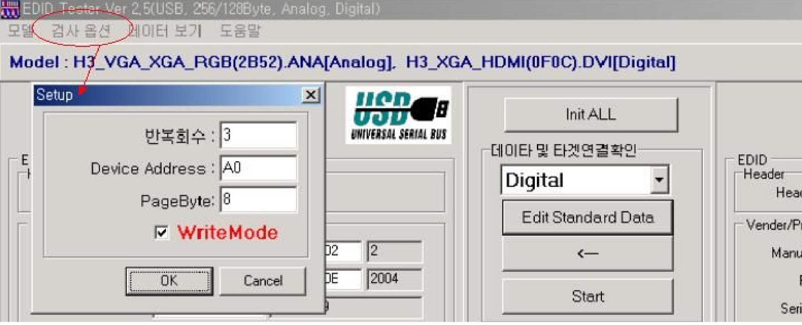
- Turn on the PC & EDID Download Jig. And Execute the S/W : EDID TESTER Ver.2.5
- Set up the S/W option.
Device Address : A0
PageByte : 8
Example Data of EDID(42PC1R-ZH)
42PC1R-ZH DDC data
of Analog-RGB (Check Sum : CE )

42PC1R-ZH
DDC data of Digital_HDMI (Check Sum
: 0B2B)


Sequence of Adjustment.
- Init the data
- Load the EDID data.( Open File : Analog ,Digital)
- Push the “Write Data & Verify” button. And confirm “Yes”.
- If the writing is finished, you will see the “ OK” message
- It is important that PP62A/C has two HDMI so digital DDC downloading must be performed two times(HDMI 1 , HDMI 2)

Main Scaler FL18668 Functions
- The FLI8668 chip has a flexible Analog Front End (AFE) with 13 configurable inputs through an analog multiplexer before the Analog to Digital Converters (ADCs).
- It also contains an embedded Multi-Standard Video Decoder. This decoder contains a digital comb filter for optimum Y/C separation. A 3D comb filter is available for optimum Y/C separation, that reduces or eliminates any artifacts due to poor Y/C separation seen on standard 2D video decoders on composite inputs, most commonly found on TV tuners.
- The FLI8668 microprocessor can process a wide range of Vertical Blanking Interval (VBI) data and display this data with the bitmap OSD processor. The microprocessor can support VBI data processing in the Main or PIP channels as well as in the background when the corresponding video stream is not present on the output stream. The VBI data slicer can extract data encoded into the VBI of the input video stream. Decoded data bytes from the VBI data slicer are stored in a memory buffer for subsequent processing by the microprocessor. The microprocessor decodes the different formats of the VBI data and passes the information to the OSD controller for output to the display controller. The VBI decoding process can run continuously in the background for inputs that contain VBI data.
- The Digital Input Port is a 48-bit data input with flexible conf iguration to support a wide range of digital sources. It consists of two 24-bit ports (PORT A and PORTB),two sets of control signals (VS,HS,ODD,etc.), and 4 input clocks. Up to 4 different inputs are supported as long as at least 2 of these inputs are 8-bit CCIR656. The digital input port can also be configured to support one 30-bit input with a second 16-bit input port. Bit 7 to 0 of PORTA can be configured as a bi-directional interface for media card applications.
- DCDi (Directional Correlation De-Interlacing) is an algorithm from Genesis Microchip’s Faroudja division, that is used to de-interlace video content (convert from interlaced to progressive scan). DCDi is known for its smooth interpolation of video content as it fills in the missing lines. Its purpose is to eliminate jagged edges (jaggies) along diagonal lines caused by interpolation, resulting in the projection of cinema-like images with exceptional picture quality.
- The FLI8668 allows a very flexible PIP display configuration whereby either the graphics or video channel may act as the PIP source to overlay over the other channel. Any one of the inputs (analog RBG, 24-bit digital, 8-bit digital, YPbPr, composite video, etc) may be multiplexed to either channel. The PIP can be from any of the AIP (Analog Input Port) 1 or 2 or DIP (Digital Input Port) 1 or 2. Single PIP allows the PIP display to be placed arbitrarily in the display window. It can be placed within the Main display, partially overlapped with Main display, or fully detached from Main display. Multiple PIPs display allows a number of PIP windows to be displayed at the same time depending on display pixel resolution. The Main and one PIP window will be running in real time. There are up to 16 PIP windows available at the same time, however only one might be acti ve. All of them should be aligned to the 4x4 grid. Default S/ W application uses multiple PIP windows to display different RF channels.
- Two LVDS channels (A and B) are available on the output of the FLI8668 to transmit data and timing information to the display device. FLI8668 directly drives the standard LVDS interface panels, supporting all standard data formats—single and dual bus, 18- or 24-bit data output. The 24-bit data may be mapped as either standard receiver formats.
- The FLI8668 has a fully programmable, true color bitmapped OSD controller capable of displaying up to 16 “tiles” or bitmap windows on the display. The individual tiles are programmable for location, size and bits per pixel, and have a precedence determining which tiles appear when overlapping occurs on the display. Tile data is stored in the external frame store memory by the OCM in either : 1, 2, 4, or 8-bit per pixel format. On-chip table registers point to the start of tiles in external memory. A programmable on-chip 256x24-bit color lookup table is provided to map the OSD pixels onto a true 24-bit color space.
- The FLI8668 on-chip microcontroller (OCM) serves as the system microcontroller. It programs the FLI8668 and manages other devices in the system such as the keypad and non-volatile RAM (NVRAM) using general-purpose input/output (GPIO) pins. The OCM can address a 22-bit address space to utilize 4 MB external ROM.