Contn:
TUNER IF / IMA / AC IN BOARD
The board contains three circuit areas of
the TV. These include AC input, Tuners and Audio. Starting with the left side
of Figure 5, the AC input is located here along with F801. The area outlined in
white is the “HOT” GND area and the components located within are not directly
related to the other circuits contain on this board. The audio amplifier IC601
is mounted on the heat sink just to the right of the AC line input area. Just
below IC601 is preamplifier IC663, BB71 is the connection to the Rear A/V
board. The remaining three components on this board are the main (H001) and sub (HY01)
tuners and the IF/Main Audio (IMA) processor H002.
Removing five screws mounted along the outside
perimeter of the board is required for board removal. However, the Rear A/V
board will need to be removed first.
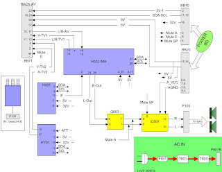
Connection BB71 to the Rear A/V board is shown. Audio
from HY01 and H002 circuits are routed through BB71 to the Rear A/V
board for switching purposes. The selected audio is
then looped back to the IMA circuit H002. The IMA (IF Main Audio) processes the
TV’s audio volume, bass, treble, etc. The IMA audio output is then sent to
preamplifier Q663 then applied to IC601 for amplification to the speakers. Mute
circuits are implemented in the preamp and amplifier circuits, details will be
covered in the troubleshooting area of the manual. The sub-audio, labeled
A-TV2, is a mono signal. The audio signal is not routed back to H002, but
applied to the monitor audio output jacks. Using sub, PIP/POP, audio feature of
this model, the user has the option of selecting the monitor jack audio to be
either main or sub audio.
Two video sources are developed on this board. Main
tuner H001 outputs an IF signal to H002. The signal is demodulated and decoded
into video and audio signals. The composite video signal is then routed from
H002 pin 7 as V-TV1 to the Rear A/V for switching purposes. The sub-picture
developed in HY01 is sent as a composite signal to the Rear A/V board for
switching as well. The gray area at the bottom of Figure 6 shows the AC IN path
block diagram, again not directly related to the audio or video.
SIGNAL / G - HYPER / DIGITAL BACK END PROCESSOR
AKA (Also Known As), the DBEP, this board
incorporates several circuits discussed in past PJTV models as “separate”
circuits. In this training module, “Signal” and “G-Hyper” along with this
board. The TV micro and DLP control
micro are located here, along with keypad and IR receiver connections.
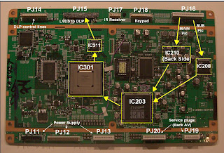
The actual board is shown, however the PC board takes
on a much different look due to metal shielding surrounding it. Disassembly of
the shields is done by removing six (6) screws holding the to halves together.
No soldering is required to remove or replace the shielding. A small pair of
needle nose is required to straighten eight (8) tabs in order to fully release
the shields. In most cases, troubleshooting can be done directly from the
connections at top and bottom without removing any shielding. The
DBEP/G-Hyper/Signal board is a replacement module, so troubleshooting to
component level in not necessary.
Arrows and IC’s outlined represent the video signal
flow. This gives a brief overview of the actual board and component locations
dealing with the signal flow.
Contd:


No comments:
Post a Comment